September 1999
Free EM Software Analyzes Spiral Inductor On Silicon
By James C. Rautio
President
Sonnet Software, Inc., 1020 Seventh North St., Suite 210,
Liverpool, NY 13088; (315) 453-3096, FAX: (315) 451-1694,
e-mail: info@sonnetusa.com,
Internet: http://www.sonnetusa.com/
SPIRAL inductors appear simple but are difficult to analyze. With the complexity of a conductive silicon (Si) substrate, the problem challenges the most advanced modern analysis tools. Amazingly, a free-of-charge electromagnetic (EM)-analysis program called Sonnet Lite can be used to provide a high-accuracy solution to this problem.
Sonnet Lite performs analysis of the three-dimensional (3D) EM fields around planar circuits. It is based on the industry-standard suite of EM software tools from Sonnet Software (Liverpool, NY). Sonnet Lite can be supplied on a compact-disc read-only memory (CD-ROM) from Sonnet® (see phone number at the end of article) for only the cost of shipping, or it can be downloaded free of charge from the company's website (also listed at the end of the article) [the download requires approximately 14-MB available hard-disk memory]. This is not a demonstration program but a fully operating (albeit scaled-down) version of Sonnet's em® program (see Microwaves & RF, August 1999, p. 152 for a review of Sonnet Lite). Sonnet Lite can handle all small-to-medium-size problems using up to 16-MB random-access memory (RAM) for a full matrix solution, up to two metal levels (and three dielectric layers), and as many as four ports. With care, a large number of problems can be solved within these constraints. The spiral inductor on Si is one of these problems.
The basic characteristic of Sonnet Lite (and its full-fledged counterpart) that makes it ideal for analyzing a spiral inductor on Si is the accuracy when conducting dielectrics are analyzed. The software is based on Fast Fourier transform (FFT) analysis. Currently, there is no accuracy-degrading numerical integration. Also, all fields in each layer are represented as a (large) sum of simple rectangular waveguide modes (the sidewalls of the conducting box containing the circuit form the rectangular waveguide). When loss is present, only the characteristic impedance and velocity of propagation of each waveguide mode need to be changed. Since these characteristics are known exactly for rectangular waveguide, substrate conductivity is included with precisely the same accuracy as seen in an equivalent lossless analysis. This is difficult to perform in analyses based upon direct numerical integration of an underlying Green's function. Thus, the only problem to overcome in analyzing an inductor on Si using Sonnet Lite is to cast the problem into a form that satisfies the analysis constraints.
Figure 1 shows the baseline inductor.
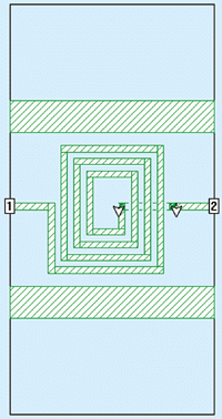
Fig 1. The baseline inductor has coplanar ground-return lines for low loss.
To reduce substrate loss, a coplanar inductor is being used. The wide conductors in the figure represent the coplanar ground strips. Ground-return current flows in these strips. Thus, the electric field from the signal line to ground need not pass through the entire Si substrate. This results in lower loss.
The inductor's transmission lines are 8 µm wide with 8-µm separation.
The ground strips are 16 µm from the edge of the inductor. The substrate
is 1000 µm thick with a relative dielectric constant of 12 and a
conductivity of 20 S/m. In addition, there is a 1-mm layer of silicon
dioxide (SiO2) with a relative dielectric constant of 4.0 on
top of the Si. Most of the inductor is on top of the SiO2
layer. The connection from the center of the inductor out is below the
SiO2 on top of the Si. A metal loss of 0.04 ![]() /square (plus
appropriate skin effects) is included.
/square (plus
appropriate skin effects) is included.
The task at hand is to simplify the model of the inductor without affecting analysis accuracy. The Sonnet software meshes only the metal surface and problem size increases rapidly with the number of subsections. Thus, the number of subsections should be reduced as much as possible.
The first way this can be performed is by making the subsection size as large as possible. With 8-µm-wide lines on 16-µm centers, this is simple enough using an 8-µm cell size. Now, all 8-µm lines are meshed one cell wide. The impact of this subsection size on analysis error is quantitatively evaluated later.
Another way that the subsection count can be reduced is by reducing the metal area. Since the coplanar ground-return lines are wide, it would be helpful if they could be eliminated from the analysis. Since Sonnet Lite places a perfectly conducting box sidewall at the edge of the substrate, the coplanar ground-return lines can be eliminated. This is performed by removing each ground strip and substituting a box sidewall in its place. Now, the ground current flows in the box sidewalls rather than in the ground strips.
As a modification, the sidewalls are placed 24 µm from the inductor (the ground strips were originally 16 µm away). Since this is a major modification, it is important to analyze the resulting effects, and an EM-analysis program supports this comparison to the original circuit conditions. Figure 3 shows a comparison of the two approaches to this analysis, with reflection parameter S11 differing by approximately 0.5 dB in the two approaches while forward transmission, S21, differs up to 2 dB, but only at the higher frequencies where S21 is down to approximately 20 dB.
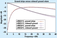
Fig 3. The inductors of Figs. 1 and 2 were compared using Sonnet Lite software. Note that the differences in S11 are approximately 0.5 dB while the differences in S21 approach 2 dB, but only at higher frequencies.
If the differences are assumed to be small compared to the design requirements, it is possible to adopt the second approach and proceed with the evaluation of the inductor of Fig. 2.
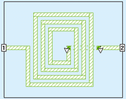
Fig 2. The inductor of Fig. 1 was modified so that the box sidewalls take the ground-return current. Removing the ground strips results in a faster analysis.
Using a typical Pentium-based personal computer (PC) running at a 450-MHz clock speed, the modified inductor of Fig. 2 can be analyzed in 1 s/frequency using only 1 MB of random-access memory (RAM). The original coplanar inductor requires 2-MB RAM and 2-s/frequency-analysis time. This may seem like a small difference at this point, but it could prove to be significant later. For those who are concerned with the 0.5-dB difference in analysis results, trade-offs can be performed using the basic inductor of Fig. 2. When the trade-offs are completed, one final analysis can be performed with all of the changes incorporated into the inductor of Fig. 1 if desired.
At this point, it is appropriate to determine the accuracy of the analysis. While suppliers of EM-analysis tools claim their programs to be accurate, the analysis errors rather than analysis accuracy are generally of interest to high-frequency engineers. It is also desirable to have a quantitative value for the error. By comparing the estimated error with the project requirements, it is possible to tell if one's trust in an analysis approach is justified.
The error mechanisms for the full version of Sonnet have been extensively investigated. In nearly all of the cases, the principal error source is error that is due to the size of the cell. A unique characteristic of this error source is the fact that the error can be cut in half by shrinking the cell size in half (with a few well-understood exceptions). Error that is due to cell size is easily evaluated. If the cell size is cut in half and the circuit is then analyzed, then the error is also cut in half.
The results of this type of a convergence analysis are shown in Fig. 4.
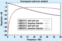
Fig 4. By cutting the cell size in half (from 8 to 4 µm), it is possible to determine error bounds. With at most 0.15-dB difference between the two results, model data should be within ±0.3 dB of the correct answer.
The original cell size is 8 µm. The second analysis uses a cell size of 4 µm with an analysis time of 6 s/frequency. The difference between the two curves is not easily seen, but is less than 0.15 dB nearly everywhere. This means that the results obtained using the 8-µm cell size should be good to approximately ±0.3 dB.
If this level of accuracy (or error) is sufficient for the needs of a particular analysis, then further modification is not necessary. But if more accurate results are needed, then an approach known as the "Richardson extrapolation" can be tried. In this technique, the total error for each data point is first determined (i.e., double the difference between the 8- and 4-µm cell-size results), and then the error is subtracted from the 8-µm answer. A spreadsheet is useful for performing a Richardson extrapolation. The results should now be accurate to approximately ±0.05 dB.
To ensure that a Richardson extrapolation is indeed providing increased levels of accuracy, a third analysis should be performed with a one-quarter-cell size. While this problem is slightly too large for the memory constraints of Sonnet Lite, it was performed in the full-featured version of Sonnet and confirmed expectations that the results are converging.
There is one exception to the ±0.3-dB error bound--the lowest-frequency data point for the forward transmission (S21) at 100 MHz appears to be incorrect.
This can happen in any EM analysis when the cell size is small compared to the wavelength. The 200-MHz point is much better than the 100-MHz point, but still appears to have some error. Due to their smaller wavelengths, frequencies that are above 200 MHz do not pose a problem. The low-frequency data are included here to show that no EM analysis can be trusted completely. Some form of convergence test should be applied in order to check the accuracy of the software.
Before attempting to reduce loss, it is helpful to perform an analysis with loss that is completely removed. A comparison of this lossless analysis with the baseline lossy inductor should provide an upper limit on how much improvement remains for the lossy inductor. In the lossless analysis, all losses (metal and substrate) were removed from the inductor model of Fig. 2. Figure 5 compares this lossless analysis with the original lossy results.
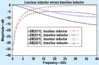
Fig 5. Comparing the loss of the baseline inductor (from Fig. 2) with the lossless version of the inductor shows that there is room for approximately 7-dB improvement at 40 GHz.
This comparison reveals approximately 7-dB loss in S21 and S11 at 40 GHz. Certainly, there is room for improvement. By comparing S-parameter data for the lossless case, the baseline case, and any case under consideration, the merits of each alternative can be quickly determined. Note that there is no need to calculate inductor quality factor (Q) which, for the complicated equivalent circuits possible with planar spiral inductors, is neither uniquely defined nor simple to calculate.
Reasoning that wider line widths should yield lower loss, modifications to the baseline inductor of Fig. 2 begin by increasing the line width from the original 8 µm to a width of 12 µm, with a 4-µm cell size for analysis (Fig. 6).
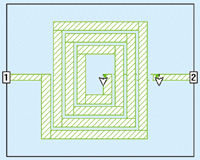
Fig 6. The line width was increased from 8 to 12 µm to evaluate the effect on inductor loss.
Figure 7 shows the results of analyzing this modified inductor model.
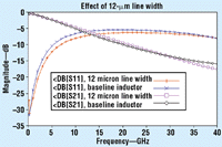
The analysis now requires 11 s/frequency. Note that the loss has generally increased. While the effect of conductor loss has undoubtedly gone down, the effect of substrate conductivity has increased. The loss drops unexpectedly around 40 GHz. The reason for this was not investigated, but may be due to a resonance above 40 GHz.
Since it did not help to cut losses by increasing line widths, perhaps it will help to decrease loss by decreasing the line widths from the nominal 8 µm to a new value of 4 µm (Fig. 8).
Fig 8. Decreasing the line width from 8 to 4 µm results in this geometry.
Figure 9 shows the analysis results (at 5 s/frequency). In these results, it is apparent that the loss has decreased substantially. If desired, this process of reducing the line width and analyzing the results can continue until the optimum line width is found.
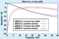
9. Decreasing line width from 8 to 4 µm results in the desired decrease in loss.
A spiral inductor on Si usually has a thin insulating layer (for example, SiO2) deposited underneath it. This reduces the effect of substrate conductivity, especially at low frequency. To reduce the loss, the insulating layer can be made thicker and/or formed with a material having a lower dielectric constant. To investigate the effects of changing the insulator thickness, it can be increased from its nominal thickness of 1 µm to a new thickness of 2 µm, then analyzed (Fig. 10).
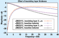
Fig 10. By increasing the thickness of the insulating layer on top of the Si substrate from 1 to 2 µm, it is possible to reduce the inductor loss substantially.
Following this, the dielectric constant of the original 1-µm-thick layer can be changed from 4.0 to 2.0 and then analyzed (Fig. 11).
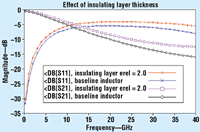
Fig 11. By decreasing the dielectric constant of the thin insulating substrate on top of the Si substrate from 4.0 to 2.0, the inductor loss is reduced substantially.
Both actions substantially reduce inductor loss at all frequencies. Now, armed with the knowledge of the relative importance of each parameter with respect to loss, and with knowledge of manufacturing and design constraints, a designer has a variety of options for realizing the lowest possible inductor losses.
To gain some further insight into this particular spiral inductor design, the inductor of Fig. 2 was analyzed with a small cell size of 0.5 µm. As a result, each line of the inductor is now 16 cells wide. Due to the size of this problem, the full-featured Sonnet software suite was used in the analysis, rather than Sonnet Lite. The resulting current distribution is shown in Fig. 12.
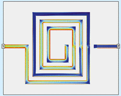
Fig 12. The current distribution for the baseline spiral inductor was analyzed with a very-fine 0.5-µm cell size. The disruption near the underpass connection to port 2 is not a numerical artifact but a real phenomenon.
Note that there is some disruption of the current distribution at the location of the underpass connection to port 2. This is common in underpass and overpass situations and is real rather than a numerical artifact.
In Fig. 12, the color red represents a current density of approximately
1200 A/m. Port 1 is excited with a 1-V source at 40 GHz connected in
series with a 50-![]() resistor. Port 2 is terminated in an impedance of 50
resistor. Port 2 is terminated in an impedance of 50 ![]() . The
analysis requires more than 12,000 subsections and 305-MB RAM. Since the
PC used in this investigation has only 256-MB RAM, substantial memory
swapping increased the analysis time to approximately 8 h. Normally, with
adequate RAM for the problem, about one hour of analysis time would be
expected.
. The
analysis requires more than 12,000 subsections and 305-MB RAM. Since the
PC used in this investigation has only 256-MB RAM, substantial memory
swapping increased the analysis time to approximately 8 h. Normally, with
adequate RAM for the problem, about one hour of analysis time would be
expected.
Although free of charge, Sonnet Lite software is quite effective for solving a difficult and troublesome problem--the analysis of a spiral inductor on a conductive Si substrate. Techniques were shown for modifying the inductor in order to reduce inductor loss and characterizing the analysis error of an EM investigation quantitatively. Richardson extrapolation was shown to be an effective method for reducing analysis error even further without resorting to the full Sonnet suite of programs. Sonnet Software, Inc., 1020 Seventh North St., Suite 210, Liverpool, NY 13088; (315) 453-3096, FAX: (315) 451-1694, e-mail: info@sonnetusa.com, Internet: http://www.sonnetusa.com/
Sonnet Lite was made possible because of work funded by DARPA under the MAFET program.