A Technology Layer allows you to define a group of objects with common properties including the metal level on which they are placed in your Sonnet project. This enables you to more easily control a large group of objects in your circuit and make changes to those objects as efficiently as possible. Technology Layers provide uses and advantages similar to using drawing layers in CAD and EDA programs.
There are three types of Technology Layers: Metal, Via and Brick.
Technology Layers have a number of uses:
One of the main uses for technology layers is to provide a mapping between drawing layers from another design environment to Sonnet specific properties, including their placement in the Sonnet stackup. By default, upon translation from another design environment to Sonnet, the name of each drawing layer is transferred to the Sonnet Technology Layer. For example, in the other design environment, if the name of the original drawing layer was Metal1, the Sonnet Technology Layer will also be called Metal1 by default. This provides continuity between the two environments. In addition, if the design is exported from Sonnet to the original or a different design environment, the layer names continue to be maintained.
If a level has a Technology Layer assigned to it, then new objects of the same type on the same level as the Technology Layer are assigned to the Technology Layer by default. For example, if you knew that every polygon you wished to add on a level should use the same metal, subsectioning and fill properties, then configuring a Metal Technology Layer with those properties would ensure that every time you add a new polygon, it would have those properties without the need for any further editing. This allows you to ensure the consistency of the new objects and add them more efficiently. In addition, using a Via Technology Layer is useful when adding a large number of vias, especially if the vias extend over multiple levels. For example, if you wished to add multiple vias from level 1 to level 4, creating a Via Technology Layer that originated on level 1 and terminated on level 4, allows you to add those vias with fewer editing steps.
Technology Layers also allow you to efficiently make changes to your circuit. Any change made to the properties of a Technology Layer is immediately applied to all the objects associated with the Technology Layer. For example, if you wish to change the material for all the metalization on one metal level, you only need to change the planar metal used for the Metal Technology Layer to which they all belong.
Technology Layers are an optional design element. While a Technology Layer, if created, must be assigned to a level in your project, it is not necessary to have a Technology Layer assigned to every level, or for a project to contain any Technology Layers at all. You may create objects, metal polygons, via polygons and dielectric bricks, that are independent and not associated with any Technology Layer. These independent elements may also be placed on a level which has a Technology Layer assigned to it. The properties of that object are not affected by any changes in the Technology Layer properties. See the appropriate properties dialog box for information on making an object independent: Metal Properties, Via Properties, or Brick Properties.
Technology Layers are created, managed and displayed using the Stackup Manager, which appears in a pane on the left hand side of the project editor. The Stackup Manager provides an overview of how the dielectric layers, metal levels and Technology Layers are organized in your circuit. For more information on the Stackup Manager, please see Stackup Manager.
All of the Technology Layers in your project may also be managed in the Tech Layers page of the Circuit Settings dialog box opened by selecting Circuit => Settings from the project editor main menu, then clicking on the Tech Layers button in the side bar menu.
As mentioned above, there are three types of Technology Layers: Metal, Via and Brick. Each type of Technology Layer uses a similar set of properties but applied to different types of objects. The set of properties for a Technology Layer include:
Please see the Technology Layer Editor for a detailed discussion of these properties.
Technology Layers are always assigned to metal levels but never to dielectric layers; however Sonnet metal levels are always attached to the dielectric layer above them. Even when using thick metal which is the same thickness as the dielectric or thicker, the Technology Layer is assigned to the metal level below the dielectric and extends upward.
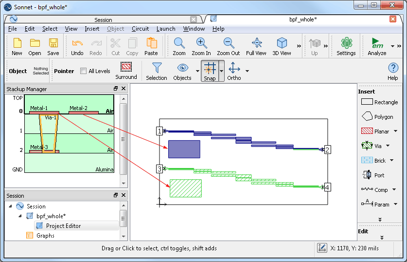
There may be multiple Technology Layers assigned to any metal level including multiple Technology Layers of the same type. For example, as pictured below, Level 0 of this circuit contains two Metal Technology Layers: Meta3 and Metal2. All of the polygons in the top filter belong to the Metal2 Technology Layer while all of the polygons in the bottom filter belong to the Metal3 Technology Layer. If you wished to move the bottom filter to level 2 of your circuit, you would be able to do so by simply reassigning the level to which the Metal3 Technology Layer was assigned.
Technology Layers may be created in four ways:
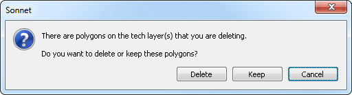
To delete a Technology Layer, right-click on the desired Technology Layer in the Stackup Manager, then select Delete Tech Layer from the pop-up menu which appears. A query box appears to ask if you wish to also delete the polygons associated with the technology layer or keep them in your project, as shown below.
To move a Technology Layer to a different level, do the following:
You may add an existing polygon to an existing Technology Layer by editing the polygon's properties.