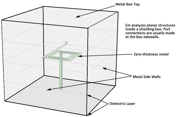
The Sonnet EM analysis is performed inside a six-sided metal box as shown above. This box contains any number of dielectric layers which are parallel to the bottom of the box. Metal polygons may be placed on levels between any or all of the dielectric layers, and vias may be used to connect the metal polygons on one level to another.
The four sidewalls of the box are lossless metal, which provide several benefits for accurate and efficient high frequency EM analysis:
As an example, a microstrip circuit can be modeled in Sonnet by creating two dielectric layers: one which represents your substrate, and one for the air above the substrate. The metal polygons for the microstrip would be placed on the metal level between these two dielectric layers. The bottom of the box is used as the ground plane for the microstrip circuit. The top and bottom of the box may have any loss, allowing you to model ground plane loss.
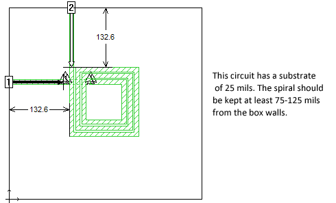
Since the four sidewalls of the box are lossless metal, any circuit metal which is close to these walls can couple to the walls - just like what would happen if you fabricated and measured a real circuit with the same box. If you do not want to model this coupling (for example, your real circuit does not have sidewalls), then you must keep the circuit metal far away from the box sidewalls. A good rule to use is at least three to five substrate thicknesses as shown below.
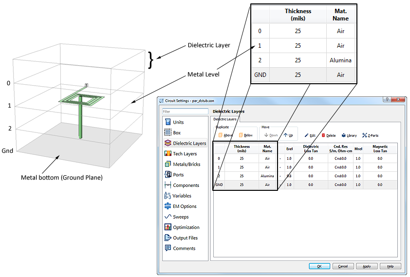
All Sonnet geometry projects are composed of two or more dielectric layers. There is no limit to the number of dielectric layers in a Sonnet geometry project, but each layer must be composed of a single dielectric material. Metal polygons are placed at the interface between any two dielectric layers and are usually modeled as zero-thickness, but can also be modeled using Sonnet’s thick metal model. Vias may also be used to connect metal polygons on one level to metal on another level.
You will use the Dielectric Layers page of the Circuit Settings dialog box (Circuit ⇒ Settings), as shown below, to add dielectrics to your circuit. Each time a new dielectric layer is added, corresponding metal level is also added to the bottom of the new dielectric layer. You may also add dielectric layers in the Stackup Manager.
This example shows a 3-D drawing of a circuit (with the z-axis exaggerated). Please note that the pictured circuit is not realistic and is used only for purposes of illustrating the box setup.