The Connectivity Checker is a tool available in the project editor which allows you to visually check for opens or shorts in your circuit. To use the Connectivity Checker, you select the command Circuit ⇒ Check Connectivity from the main menu of the project editor. Once the checker is invoked you can click on any metal or via polygon in the circuit to see the polygons to which it is electrically connected or any shorts created by the polygon. The process is detailed below.
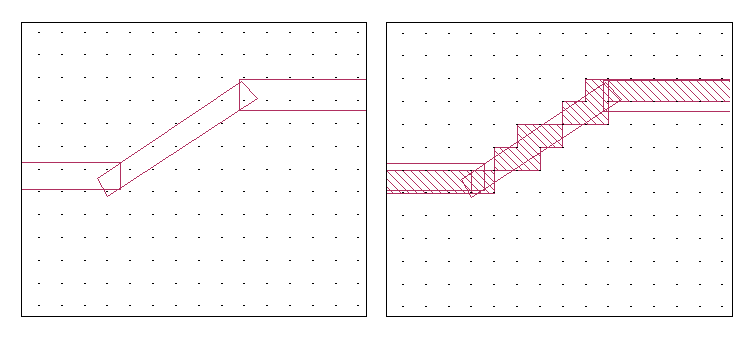
The Connectivity checker uses the cell fill when checking the connectivity. The cell fill represents the actual metalization analyzed by the analysis engine, em, and may differ from the polygons input by the user, or translated into Sonnet from another tool. Using the Connectivity Checker can identify problems created by the differences between the input polygons and the cell fill. An example where the cell fill creates an open is shown below. The circuit is shown on the left with the cell fill turned off so you see only the input polygons. On the right is a view of the input polygons with the cell fill turned on. The input polygons provide a connected electrical path, but because of the staircase fill, the solver would treat this as an open circuit.
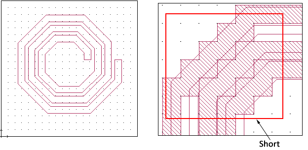
Cell fill can also create an undesired short as shown below.
An example circuit, connectivity, will be used to explain the operation of the Connectivity Checker and is shown below. This example file can be found in the Sonnet example files. You may access the Sonnet Example browser by selecting Help ⇒ Browse Examples from the menu of any Sonnet application. For instructions on using the Example Browser, please click on the Help button in the Example Browser window.
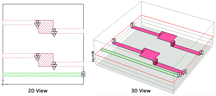
When you invoke the Connectivity Checker, all the polygons and vias in the 2D view are displayed with grey fill while the circuit in the 3D view is displayed as a wire frame as illustrated below.
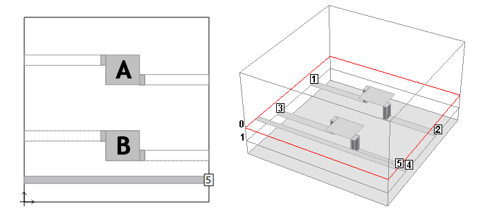
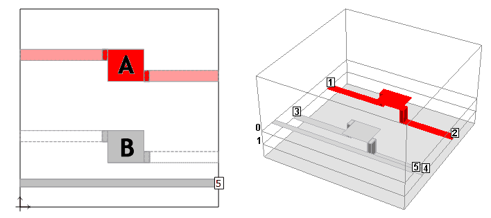
When you click on a polygon, it and all the polygons to which it is electrically connected are highlighted in red. If there are polygons or vias that are connected on another level, they are highlighted in a lighter red. In the graphic below, polygon A was selected. The path starting at Port 1 and extending to Port 2 was highlighted. As noted earlier, the feedlines are on another level from the center polygon so in the 2D view they are light red. The whole path is highlighted in red in the 3D view.
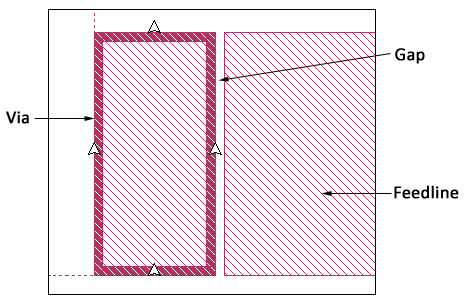
The gap between the via and the feedline is not discernible at full view, but zooming in on the connection shows that it exists.
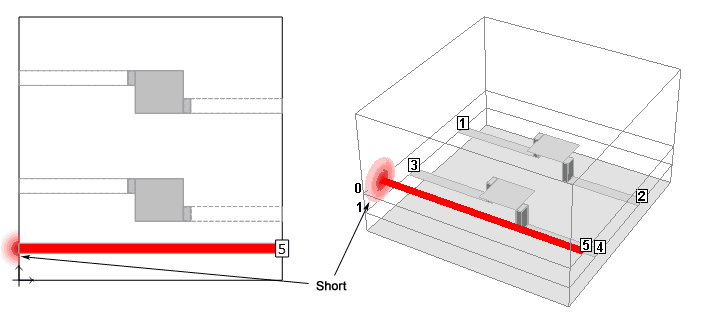
In the next illustration, the trace at the bottom of the circuit is selected. There is a “bloom” shown at one end of the line. Since there is no port on the box wall, the trace is shorted to ground; this is indicated by the “bloom.” The other end of the polygon has a box wall port. Ports are always considered opens which is why there is no bloom on the other end of the polygon.
Once you are finished using the Connectivity Checker, press the Escape key to exit this mode and return to Edit mode.
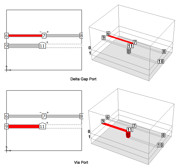
As mentioned earlier, ports are always considered an open circuit. This includes both delta gap ports and via ports as pictured below. For both the delta gap port, shown on the top in 2D and 3D views, and the via port pictured on the bottom, the electrical connection only extends to the port.
A complete list of geometry elements and how they are treated by the connectivity checker is provided below.