The following restrictions apply to the placement of Components in your circuit:
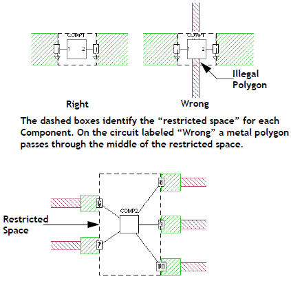
- No objects may be placed within the “restricted space” in the interior of the Component.
Metal polygons, vias, or dielectric bricks may not be present in the rectangular area defined by the port locations and the terminal width, as illustrated below. The bottom circuit shows the restricted area in a multiport Component.
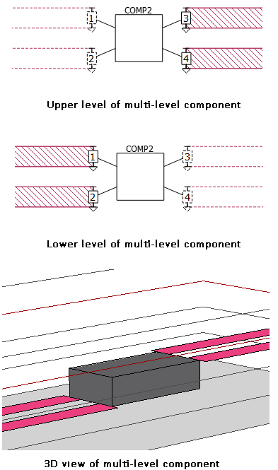
- Components may be multi-level with the terminals occurring on different metal levels.
Ports may be placed on different levels as long as the other rules are observed. An example of a multi-level component is shown below in both the 2D and 3D view.
- Components whose ground references are defined as the Sonnet box require direct access to the Sonnet top or bottom cover.
The analysis engine determines the most efficient direction the ground via extends taking into consideration both the distance and the loss of the box top or bottom. When using this type of ground, you must make sure that there is a clear path with no metal on other levels interfering with the path to either the box top or box bottom.
In addition, the box top or bottom should not have loss greater than 50 ohms/sq. If the loss is too high on both the box top or bottom for a ground via from the Component to be attached, the analysis engine issues an error message.
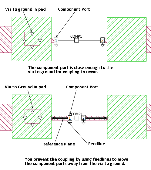
- Nearby objects should be placed so that coupling between the Component and the object does not occur.
Metal polygons, vias, or dielectric bricks which couple to the Component ports may decrease the accuracy of the analysis as shown below.
It can be helpful to add feedlines to all the terminals of a component, then use reference planes to remove the effect of the feedlines. This allows you to place the component ports and any ground reference vias far enough away from other circuit elements to prevent coupling. Note that in order to use reference planes for a component port, your ground reference cannot be set to "Floating."
In the illustration below, the top circuit places the component port close enough to the via to ground in the pad for coupling to occur. In the bottom circuit, feedlines have been added to move the component ports further away in order to prevent any coupling to the via. Reference planes are set for the component ports to remove the effects of the feedlines during the de-embedding process.
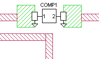
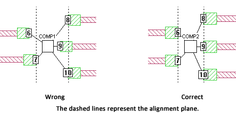
- Multiple ports on the same side of a Component should be aligned.
In the illustration below, the ports on Comp1 are placed incorrectly and will produce an error during an analysis. The ports on comp2 are placed correctly.
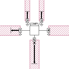
- Reference planes must be the same length for each side of a Component.
Note that the reference planes for ports 2 and 3 in the illustration below are the same length. It is important that these ports share a reference plane since the feedlines are close enough that coupling between them becomes a factor and needs to be removed during de-embedding. However, reference planes can be different lengths for each side of the “component rectangle” as shown by ports 1, 4 and 5 below. Since these ports are on different sides of the component, their reference planes are independent from ports on other sides.
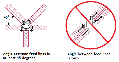
- The angle between feedlines of diagonal components should be at least 45 degrees.
This means you should never have parallel diagonal feedlines on a single side of a component.