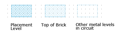
Once a dielectric brick has been created in the project editor, it is possible to “see” the brick from both the circuit layer where the base of the brick is located and the circuit layer where the top of the brick is located. On both levels, you will see a polygon which defines the cross-sectional shape of the dielectric brick. The brightness of the polygon, however, will vary. When you are on the top level, you will see a “dim” polygon; on the base level you will see a “bright” polygon.
Only the outline of the dielectric brick is visible from levels other than the origination and termination of the dielectric brick.
Note that while it is possible to “see” a brick from two different circuit levels, “selecting” a brick, for cutting, copying, moving, changing attributes, etc., can only be done from the circuit level where the base of the brick is located if you are in Single layer edit mode. The polygon can be selected on either level if you are in multilayer select.
Finally, it is possible to turn the display of dielectric bricks “on” or “off” in the project editor. You select View ⇒ View Options from the main menu of the project editor, then click on Visibility in the side bar menu of the View Options dialog box which appears on your display.
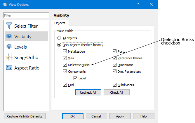
Click on the Only Objects Checked Below radio button to enable the object choices, then click on the Dielectric Bricks checkbox to turn off the display of the bricks.
This will make any bricks present in the circuit invisible and unselectable, but does not remove them from the circuit. The dielectric bricks can be turned back “on” by selecting the Dielectric Bricks checkbox or the All Objects radio button.
Occasionally, when a circuit contains many layers, with overlapping metal polygons and dielectric bricks, it may be somewhat difficult to distinguish the metal polygons and dielectric bricks from one another. The ability to turn dielectric bricks “off” usually makes it easier to view such circuits.