Connectivity Checker
The Connectivity Checker is a tool available in the Project Editor and allows you to visually check your circuit for open or short circuits. To use the Connectivity Checker, select Circuit > Check Connectivity from the main menu of the Project Editor. Once the checker is invoked, click any metal or via polygon in the circuit. This will allow you to see the polygons to which it is electrically connected or any short circuits created by the polygon. The process is detailed below.
The Connectivity Checker uses the Snapped Fill when checking the connectivity. The Snapped Fill represents the actual subsections analyzed by the EM solver, and may differ from the polygons input by the user. Using the Connectivity Checker can identify problems created by differences between the input polygons and the Snapped Fill. An example where the Snapped Fill creates an open circuit is shown below. The circuit is shown on the left with the Snapped Fill turned off, so only the input polygons are visible. On the right is a view of the input polygons with the Snapped Fill turned on. The input polygons provide a connected electrical path, but because of the rectangular meshing, the EM solver would treat this as an open circuit.
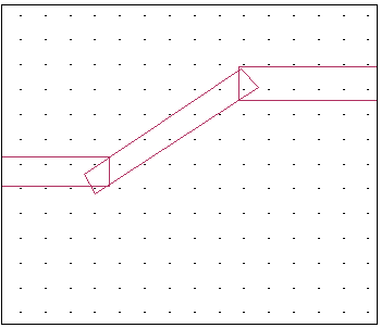
Snapped Fill off
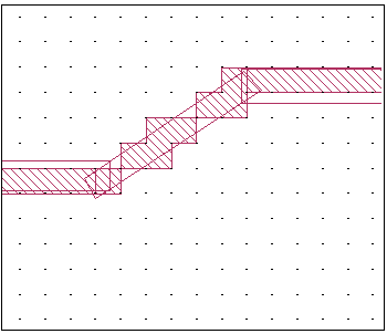
Snapped Fill on
Additionally, the Snapped Fill can create an undesired short circuit as shown below. The turns of the inductor within the red rectangle are shorted together due to the cell size being larger than the gap between the turns.
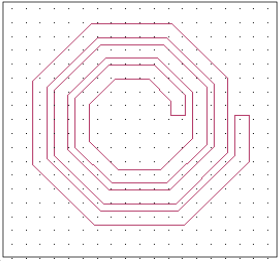
Snapped Fill off
Snapped Fill on (zoomed up)
When you invoke the Connectivity Checker, all the polygons and vias are displayed with gray fill as illustrated below. Two polygons are labeled with the letters "A" and "B" for future discussion.
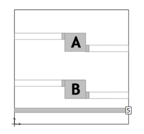
Initial 2D View
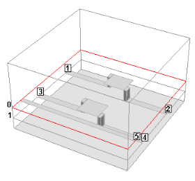
Initial 3D View
When you select a polygon, it will be highlighted in red. Polygons that are electrically connected to the selected polygon will also be highlighted in red. Also, any polygon on another level that is electrically connected to the selected polygon will be highlighted in a lighter red. In the pictures below, polygon A was selected.
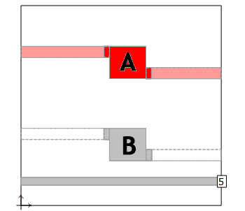
Polygon A is selected (2D)
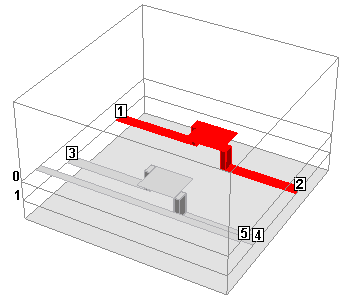
Polygon A is selected (3D)
In the next illustration, the trace at the bottom of the circuit is selected. A bloom is shown at one end of the line. Since there is no port on the box wall, the trace is shorted to ground; this is indicated by the bloom. The other end of the polygon has a box wall port. Ports are always considered open circuits which is why there is no bloom on the other end of the polygon.
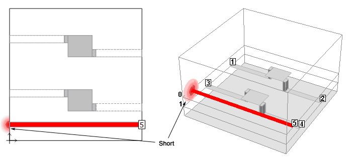
A bloom indicates a short circuit
Once you are finished using the Connectivity Checker, press the Esc key to exit this mode and return to Edit mode.
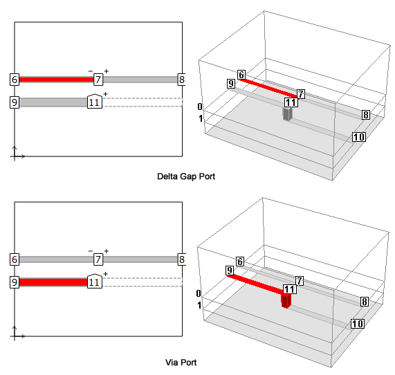
As mentioned earlier, ports are always considered an open circuit. This includes both Delta Gap ports and via ports as pictured below. For both the Delta Gap port, shown on the top in 2D and 3D views, and the via port pictured on the bottom, the electrical connection only extends to the port.
 A list of geometry elements and how they are treated by the Connectivity Checker is provided below.
- Ports: All port types are treated as an open circuit.
- Components: Components are treated as an open circuit.
- Dielectric Bricks: Dielectric Bricks are treated as an open circuit.
- Lossy Metal: Lossy Metal is treated as a closed circuit. The loss of the metal is not taken into account by the Connectivity Checker.