The Volume via loss model is the most commonly used model because the values you specify are directly related to the physical properties of the via. With the volume model, you enter a conductivity and Volume Properties. The Volume Properties section allows you to model both hollow and solid vias.
Specify Using: You may chose to define your metal loss using Conductivity, Resistivity, Sheet Resistance at DC or Resistance Per Via. You should use whichever value you have available for your metal. Select which value you wish to use from this drop list. The dialog box is updated to include a text entry box for whichever choice you make in the drop list; the units are displayed to the right of the text entry box. You may use a variable to define the conductivity, resistivity sheet resistance at DC and resistance per via.
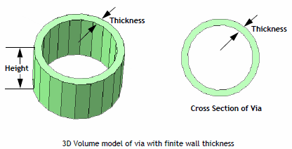
Hollow: If your vias are hollow, you enter the wall thickness of your vias. The wall thickness and the shape of each via polygon are used to determine the cross-sectional area used for the loss calculations. In the illustration below, a 3D view of the via is shown on the left, with the cross sectional area shown on the right.
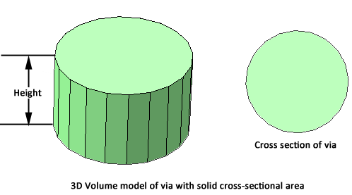
Solid: If your via is solid, you select the "Solid" radio button. The complete area of the via polygon is used for the loss calculations. In the picture below, the cross sectional area is the area of the circle.
Note that defining your Volume Properties as either Wall Thickness or Solid does not affect the subsectioning of the via or how the via appears in the project editor.
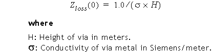
The vertical DC impedance of a via using the volume loss model is a resistance based on its physical characteristics:

where
H: Height of via in meters.
s: Conductivity of via metal in Siemens/meter.
A: Cross-sectional area of via based on wall thickness or solid setting.
At RF, the equation is too complex to show here, but is the volumetric equivalent of the surface impedance equation used by Sonnet for planar metal. This equation includes the skin effect, resulting in a smooth transition from DC to high frequencies , and is described in detail in the following article:
James C. Rautio and Veysel Demir, “Microstrip Conductor Loss Models for Electromagnetic Analysis,” IEEE Transactions on Microwave Theory and Techniques, Vol. 51, No. 3, March 2003, pp. 915 - 921.
The loss may also be defined by using the Resistance per Via. Resistance per Via for the volume model represents the total resistance in Ohms of the via polygon in the vertical (Z) direction. This resistance is constant with frequency. If the via polygon extends over more than one dielectric layer in the Z-direction, then the total specified resistance is apportioned to each layer according to the thickness of each layer. For example, if the specified RPV for a via polygon is 3.0 Ohms, and if the via polygon extends from the top of dielectric layer 1 (10 um thick) to the bottom of dielectric layer 2 (20 um thick), then 1 Ohm is apportioned to dielectric layer 1 and 2 Ohms is apportioned to dielectric layer 2.
When you are using the Volume Loss model (solid) for bar vias (mesh is set to Bar), then the horizontal DC loss in ohms/square is calculated as follows:
The horizontal DC loss for other types of fill is geometry and meshing dependent so it is not possible to provide an equation.