The current density viewer allows you to view the current density distribution in your circuit. When you select the Compute Currents option in the Em Options dialog box in the project editor, em calculates current density data for all the metal levels in your circuit. When you have thick metal in your circuit which ends in the interior of a dielectric layer, then the current density viewer creates "sublevels" of metal to display all the current density data.
For instance, you have a circuit with 3 mil thick metal using the default 2 sheets placed on metal level #1 below a 25 mil dielectric layer as pictured below. The top of the thick metal structure is placed in the interior of the dielectric layer. The current density viewer displays levels 1b and 1a, where 1b is the metal level on which the thick metal was drawn and 1a is the top of the thick metal structure embedded in the dielectric layer.
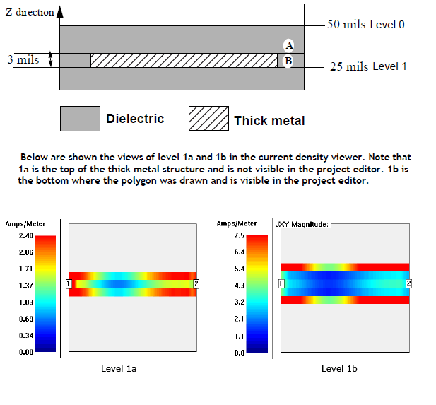
The current density viewer creates as many “sublevels” as are needed. For example, a physically thick metal which is defined as having 4 sheets placed on level 2 would appear in the current density viewer as 2a, 2b, 2c and 2d with 2a being the top of the thick metal structure and 2d being the bottom drawn on level 2.