To create a thick metal polygon in your circuit, you must first define a metal type using the Thick Metal model, then apply that metal type to the polygon in your circuit. This creates a thick metal polygon which extends upwards (toward the box top) from the metal level on which it is created. To do this, perform the following:
- In the project editor, select Circuit - Settings from the main menu.
The Circuit Settings dialog box appears on your display.
- Click on Metals/Bricks in the side bar menu of the Circuit Settings dialog box.
The appearance of the dialog box is updated to display the Metals/Bricks page.
- If it is not already selected, click on the Planar Metal tab in the Metals/Bricks page.
The appearance of the dialog box is updated to display the Planar Metals. Any planar metals that are defined in the project appear in the displayed list.
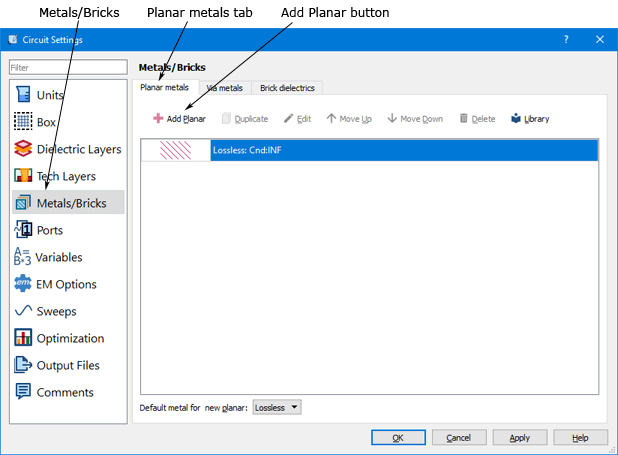
- Click on the Add Planar button
 in the Planar Metals tab.
The Planar Metal Editor dialog box appears on your display.
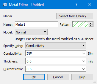
- Select Thick Metal Model from the Model drop list in the Metal Editor dialog box.
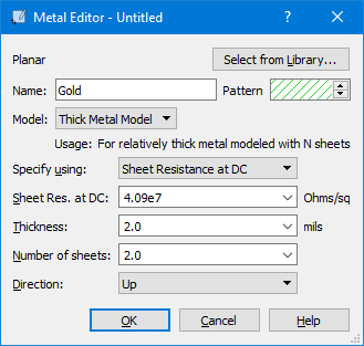
This updates the dialog box with the text entry boxes for the four parameters needed for the thick metal model: Thickness, Number of Sheets, Direction and a fourth parameter which is set by selecting either Conductivity, Resistivity, or Sheet Resistance at DC from the Specify Using drop list. The default is Conductivity. The example below uses the Sheet Resistance at DC. Note that this is the overall Sheet Resistance of the metal, and is not related to the number of sheets being used. For more information on Conductivity, Resistivity, and Sheet Resistance at DC, please see Conductivity, Resistivity, or Sheet Resistance at DC.
The direction parameter defines whether the metal extends upward into the dielectric layer above (the default setting) or extends downward into the dielectric layer below.
- Enter the four parameters in the appropriate text entry boxes.
- If you do not wish to use the default metal name, enter the desired name for the metal type in the Name text entry box.
For this example, the name of the metal type is "Gold." The Metal Editor dialog box should appear similar to the picture below.
- Click on the OK button to close the Planar Metal Editor dialog box and apply the changes.
The Metal Types dialog box is updated with the new metal type. Note that the new metal type entry says "unused" since it has not yet been used for any polygons in the project.

- Click on the OK button to close the Circuit Settings dialog box.
The thick metal is now available to use in your project.
- Enter the desired polygon, then double-click on the polygon to open the Planar Polygon Properties dialog box.
- Select the thick metal model metal type from the Planar drop list in the Planar Polygon Properties dialog box.
This will apply the metal type which uses thick metal to the selected polygon. In this case, since the Direction selected was “Up,” the thick metal extends upwards from the level on which the polygon was drawn. If you had selected “Down” for the direction, the metal would have extended downward from the metal level.

- Click on the OK button to close the Planar Polygon Properties dialog box and apply the changes.
The fill pattern of the polygon changes to the fill pattern used by the thick metal. If the thick metal polygon is thicker than the dielectric layer(s) above it, the polygon also appears on metal levels above.
You may also assign a thick metal model metal type to a Metal Technology Layer.