Metal plating is a commonly used finishing process in circuit fabrication. Printed Circuit Boards (PCBs) often have plated finishes to protect the three exposed sides of copper traces from oxidation. Lossy metal plating, such as nickel, can have a significant negative effect on the high frequency loss of a circuit and can be essential to capture in a model.
It is possible to model metal plating which coats the three exposed sides of bare metal using multiple Thick Metal Types. To model the plating, you add a Thick Metal polygon on top of the base metal polygon to represent top plating and narrow Thick Metal polygons along the edges, to represent edge plating.1
Procedure Outline
The basic procedure for modeling metal plating of the three exposed surfaces is below, followed by an example of modeling plated metal for a simple through line.
- Set the cell size of the project to be less than or equal to the thickness of the plating you wish to model. For Manhattan traces, using a cell size equal to the thickness of the plating is usually sufficient, but for circuits with diagonal or curved structures, a smaller cell size is required.
- Specify a Thick Metal type for the base metal, a second Thick Metal type for the top metal plating, and a third Thick Metal type for the edge plating.
- The thickness of the Dielectric Layer in which the base metal and edge plating metal are placed should be specified using the same thickness as the base metal. This will create a metal level on top of the base metal trace where you can add the top metal plating.
- Specify the desired Technology Layers in the Stackup Manager. Using Technology Layers is optional, but they can help you understand the modified stackup at a glance.
- Create the layout of the base metal (unplated) polygons.
- Draw narrow polygons alongside the base metal edges representing the edge plating.
- Draw the top metal plating polygons. You should be able to copy, then paste, the base metal polygons and the edge plating polygons created in the previous two steps. Ensure the pasted polygons are then set to the plated metal properties. If you are using Tech Layers this is done automatically, but if not, you will need to change the metal type of the polygons.
PCB Through Line Example
NOTE: The example project discussed below is delivered with your software and may be accessed through the Example Browser. The name of the example is "plated_thruline."
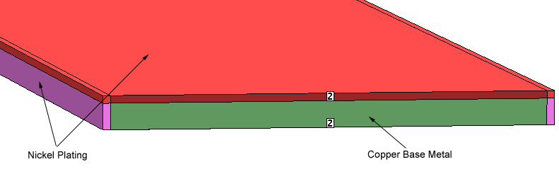
The example project, containing a nickel plated copper trace is shown in the 3D view below: The plating is modeled as covering the three exposed surfaces of the trace.
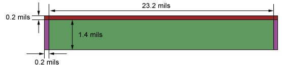
A cross-sectional view with the dimensions is shown below. Note that the drawing is not drawn to scale for clarity.
The next two figures contain 2D top views looking straight down on the base metal of the through line (metal level 2) and on the top plating metal (metal level 1) respectively. A view of the Stackup Manager with the metal level highlighted is shown in each figure. Note that ports are added on both metal levels.
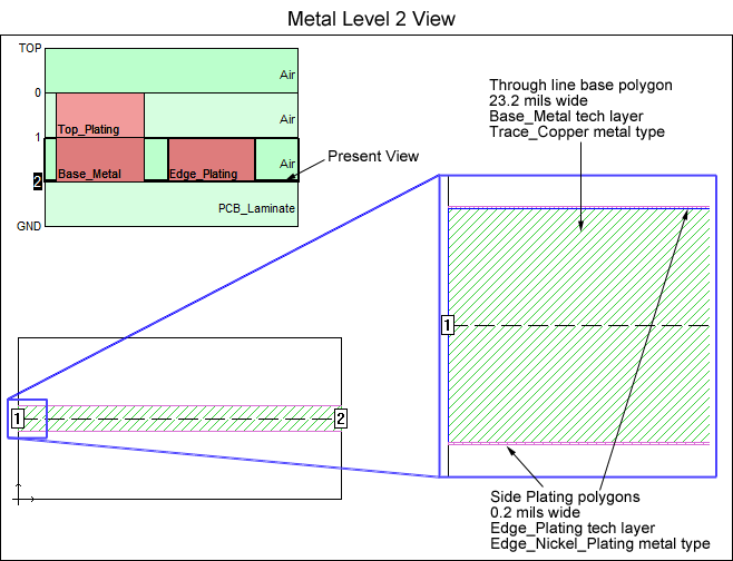
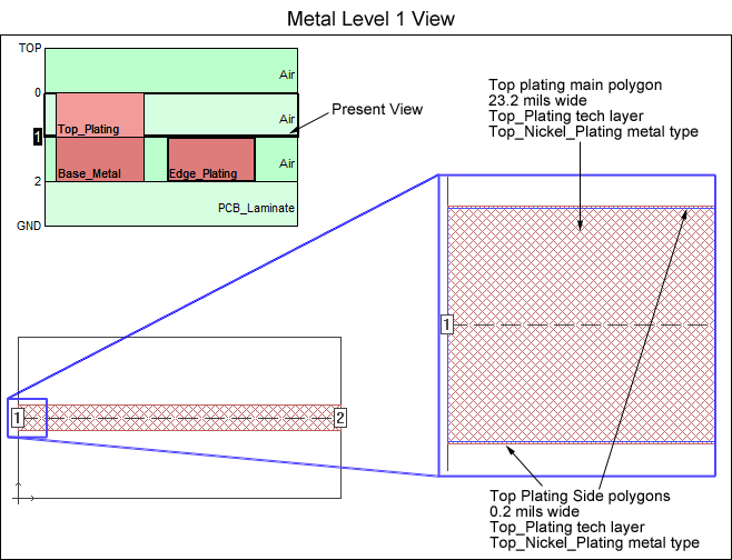
The metal types used in this model are all Thick Metal as shown below:
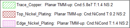
The nickel conductivity value is set to the variable "NiCond," which has a value of 5e5 S/m. This value was found by experimentation to match measured data for a physical PCB through line. The nickel used in PCB plating is typically a nickel phosphorus alloy and can vary. The best practice is to perform your own benchmark and determine an appropriate nickel conductivity value for your process.
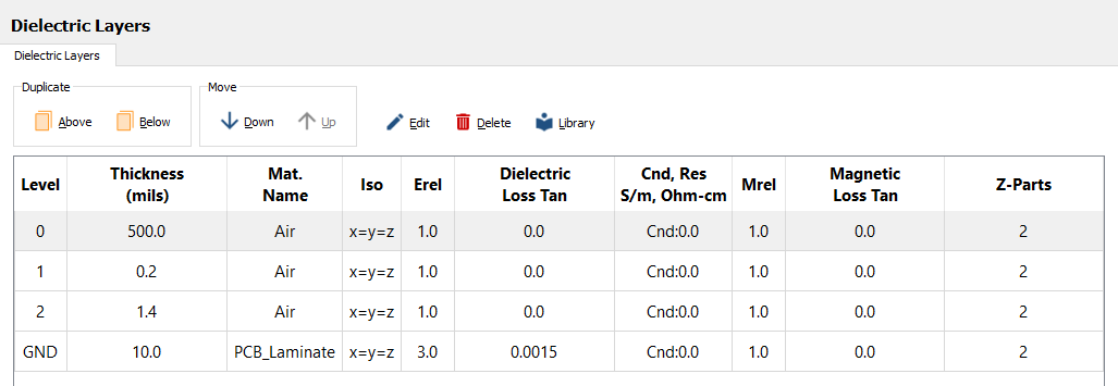
The Dielectric Layers page for this example is shown below. The base metal and edge plating metal are placed in the 1.4 mil Air dielectric layer (see the Stackup Manager in the illustrations above). This dielectric layer is the same thickness as the base metal. The top metal plating is placed in the 0.2 mil Air dielectric layer which places it directly on top of the base metal. This dielectric layer is the same thickness as the plating metal.
Special Considerations when Modeling Plating
- This technique is only suitable to use with standard Boxwall Ports. Applying internal ports, such as Co-Calibrated Ports, could lead to errors.
- This technique is only suitable to use with staircase mesh It is not compatible with conformal mesh or diagonal fill.
- This technique is most accurate when the base metal is much wider than the total trace thickness.
- You can use this same method to simulate the plating on larger, more complex circuits than the simple through line example shown above. However, due to the small cell size necessary to model the plating, an analysis of such a circuit could be impractical. If you encounter this scenario, you could use the plated through line model results to find an effective conductivity value you can apply to a new, single Thick Metal type in your larger circuit.
- This example describes a common scenario wherein the entire base metal trace is plated on all exposed surfaces. This approach can still be used if you are working with a different plating finish, with limited plating areas. You would match the plated areas in the model to those in your physical part. For example, if only the top surface is plated in your physical part, you can omit the “Edge_Plating” Technology Layer and associated polygons from the model.
- Nickel plating is typically not the final plating finish. Often a very thin topcoat of gold is added, such as in an ENIG (Electroless Nickel Immersion Gold) process. Testing has shown that this top gold plating has a minimal effect on the insertion loss until relatively high frequencies. A second plating metal can be added to the model, at a substantially higher computational cost.
1Brian Rautio, John Coonrod, "An Efficient EM Simulation Model for ENIG Plated Metal Finishes Including Conductor Side-Wall Plating Verified with Physical Measurement from 1 to 50 GHz," IMWS-5G 2018, August 30th - 31st 2018, Dublin, Ireland.