Tutorial: Finalize Your Project
In this part of the tutorial, you will finalize your project, making it ready to be analyzed by the EM solver.
Open Example File
This page assumes you have already performed the previous steps of this tutorial and have saved your project file as part2_geometry.sonx. If you have not, you may use the example file provided with your Sonnet installation. Click the triangle below to expand the instructions for obtaining the example file.
Obtaining the Example FileObtaining the Example File
To obtain the example file, follow these instructions.
Select Help > Browse Examples from any Sonnet tab.
The Example Browser opens.
Find the Getting Started Tutorial and select it.
You may use the search box or scroll down until you see the Getting Started Tutorial example.
Click the Save button at the bottom of the Example Browser window.
A Save Example window opens with a list of files that will be saved.
Enter or browse for the folder where you wish to place the example files.
Choose a location you can remember.
Click the Save button.
The example files are saved to the specified folder.
Click the Close button.
The Example Browser closes.
If you have not done so already, open the file, part2_geometry.sonx.
Navigating within Your Stackup
The main portion of the Project Editor shows a 2D view of your circuit. By default, polygons on the present level are shown with an outline and a fill pattern, and polygons on other levels are shown using dashed outlines. You may change levels using any of the following methods:
- Levels toolbar: Click the Level Up
 or Level Down
  buttons in the Levels toolbar, or select the level number from the drop-down list adjacent to the Level Up and Level Down buttons.
 - Keyboard: Press the Up or Down arrows on your keyboard.
- Stackup Manager: Click the Tech Layer symbol in the Stackup Manager. When a Tech Layer symbol is selected, the level changes to the level of the selected Tech Layer. In addition, adding a polygon while a Tech Layer is selected will place the polygon on the selected Tech Layer.
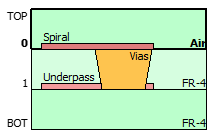
Stackup Manager with Underpass Tech Layer selected
Navigating your stackup is a task you will use often. Therefore, you should become familiar with each method.
Use the Levels toolbar to navigate to levels 0, 1, and BOT of your stackup.
You should notice that when level 0 is selected, the Spiral metal is completely visible and only a dashed outline of the Underpass metal is displayed. When level 1 is selected, the Underpass metal is completely visible and only a dashed outline of the Spiral metal is displayed. The BOT level represents the bottom cover of the Analysis Box and both Spiral and Underpass metal are represented by dashed lines because neither one is on the BOT level.
Use the Up and Down arrows on your keyboard to navigate to the different levels of your stackup.
Using the Up and Down arrows does the same thing as using the Levels toolbar.
Use the Stackup Manager to select each Tech Layer in your stackup.
You may right-click on a Tech Layer symbol for more options, such as selecting all polygons assigned to the selected Tech Layer.
Add Feedlines
Feed transmission lines are required in many circuits to connect ports to the device under test (DUT). In this tutorial, you will need to create two feedlines to connect the spiral inductor to the Analysis Box walls. Box-wall ports will then be added to the ends of the feedlines.
In the Stackup Manager, select the Spiral Tech Layer.
The Spiral Tech Layer symbol is highlighted, and level 0 is displayed in the main Project Editor window. Selecting the Spiral Tech Layer allows you to add the feedline polygons to the Spiral Tech Layer.
Select Insert > Draw Rectangle.
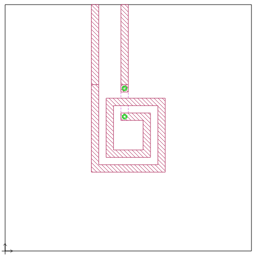
Draw a rectangle from the top edge of the left feed of the spiral inductor to the Analysis Box wall as shown in the animation below.
You may find it convenient to zoom in on the area (using the various zoom toolbar buttons) before attempting to draw the rectangle.
Draw another rectangle from the edge of the via pad to the Analysis Box wall using the same procedure as before.
When finished, your circuit should look like the image below:
Add Ports
The next step is to add ports to the two feedlines you just added. The most common type of port is a Box-wall port and will be used here. For more details about Sonnet ports, see Introduction to Ports
Select Insert > Port.
Your cursor changes to indicate you are in Add Port mode.
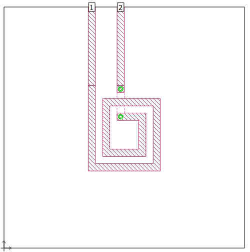
Click the top edge of the left feedline.
Port 1 is added to the left feedline.
Using the same method, add a port to the top edge of the right feedline.
Port 2 is added to the right feedline. Your circuit should look like the image below:
Add Reference Planes
Adding the feedlines was necessary to connect the spiral inductor to the ports on the Analysis Box wall. However, if the length of a feedline is not electrically short, unwanted phase (and possibly loss) will be added to the results. If the impedance of the transmission line differs from the normalizing impedance of the S-parameters (usually 50 ohms), the results may contain an additional error. Thus, if you are interested in only the behavior of the spiral inductor, the affect of the feedlines needs to be negated during the de-embedding portion of the EM analysis. The process of negating lengths of transmission line during de-embedding is known as "shifting reference planes". In this step of the tutorial, you will add reference planes to ports 1 and 2.
Select port 1 or port 2.
Since both ports are on the same Analysis Box wall, they will share a reference plane.
Select Object > Port Properties.
The Port Properties dialog box opens for the port you selected.
You may also double-click a port to edit its properties.
In the Reference Plane drop-down list, select Linked.
A linked reference plane is a reference plane that is linked to a vertex of a polygon. When that vertex on the polygon moves, as part of a reshape or a new value for a parameter, the length of the reference plane also changes. Linked reference planes are indicated by the outline of an arrow.
Click the Use Mouse button.
The Port Properties dialog box temporarily disappears and your cursor changes. The software is waiting for you to select a vertex for the linked reference plane.
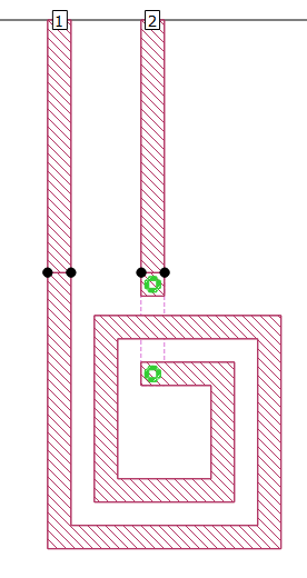
Select any of the vertices at the intersection of the feedline and the spiral inductor.
You may select any of the vertices indicated below with a black dot:
After selecting a vertex, the Port Properties box reappears.
Click OK to save your changes and exit the Port Properties dialog box.
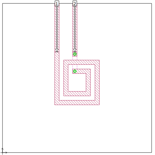
Arrows indicate the new reference planes. Since the port was previously selected, the port and its reference plane are highlighted, indicating they are still selected.
Click any blank area in your circuit to unselect the port and reference plane.
Your circuit should now look like the image below:
As a short-cut, you can select Insert > Add Feedline. This extends a feedline from the polygon edge to the Analysis Box wall and adds a Box-wall port and a linked reference plane. See Insert Feedline for more details.
3D View
You may open a 3D View of your circuit.
Select View > 3D Geometry View.
A three dimensional view of your circuit is opened in a new tab.
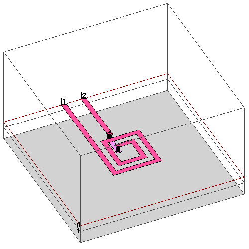
Click and drag your cursor to rotate the view.
The initial mode of the 3D view is the rotate mode. Other modes, such as zoom and pan may be accessed using the View menu or toolbar.
When finished, click the close icon  on the 3D View tab to close it.
The tab closes, and the 2D Geometry View tab becomes the active tab.
You may also use the middle mouse button or the menu Window > Close Tab to close a tab.
Save Your Progress
Select File > Save As and save the project as part3_finalized.sonx.
Your project is now ready to be analyzed by the EM solver. Click the Next button below to continue.