Via Tech Layers
Via polygons can be used to connect metal on any level in a circuit to metal on any other level. They are commonly used to model vias to ground, connections to air bridges, and can even be used to approximate wirebonds.
Via polygons use a uniform distribution of current along their height and thus are not intended to be used to model electrically long vertical structures. Therefore, the height of the via polygon should be a small fraction of a wavelength. If you need to make a connection through an electrically thick dielectric, you may need to divide the dielectric into multiple layers to achieve an accurate analysis.
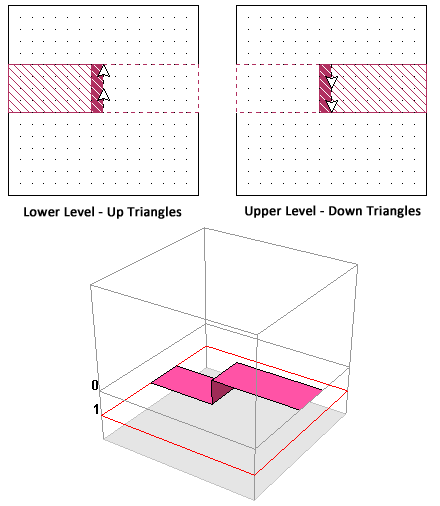
When viewed in the Project Editor's 2D view, via polygons show a "down" and/or "up" via symbol as shown below.
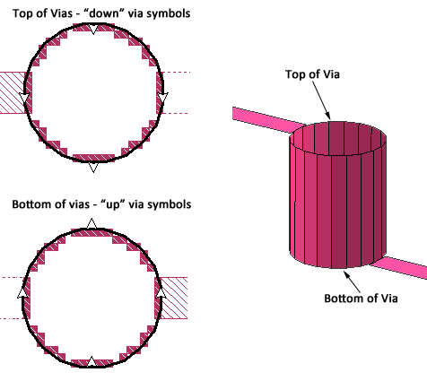
When you are viewing the level at the bottom of the via, the "up" via symbol is displayed to indicate that the via extends upward from the present level. Similarly, if you are viewing the level at the top of the via, the "down" via symbol indicates that the via extends downward from the present level. If you are viewing an intermediate level, both symbols are displayed.
Creating Vias
To create a via, follow these steps:
Select the desired Via Tech Layer in the Stackup Manager.
If you have not already created a Via Tech Layer yet, you will be prompted to create one during the next step.
Select Insert > Via followed by the method which you wish to create the via.
Depending on which method you chose, and if you have not already selected a Tech Layer, you will be given a choice of creating a new one or using an existing Tech Layer.
Vias must be placed on a Via Tech Layer. If you wish to add a Via Tech Layer, select Circuit > Settings > [Tech Layers] and click the Add Via button. Similarly, if you wish to edit an existing Tech Layer, select Circuit > Settings > [Tech Layers], select the Tech Layer, and click the Edit button. Alternatively, you may use the Stackup Manager to create or edit a Tech Layer. After doing any of these methods, the Via Tech Layer Properties dialog box will launch.
Via Tech Layer Properties
Via Tech Layers group via polygons that share the same properties, including their beginning and ending locations. Any change made to the properties of a Via Tech Layer is immediately applied to all the polygons assigned to that Tech Layer (see Inherit vs. Override for an exception).
To add a Via Tech Layer, select Circuit > Settings > [Tech Layers], select the Tech Layers tab and click the Add Via button. The Tech Layers Properties dialog box will launch. Alternatively, if you wish to edit an existing Via Tech Layer, select select the Via Tech Layer you wish to edit, and click the Edit button. You may also edit a Tech Layer using the Stackup Manager.
The Tech Layer Properties dialog box allows you to specify the following information:
Name: The name must be unique, is case sensitive, and cannot contain any of the following characters:
Begin/End: The Begin and End fields determine the locations where the Via Tech Layer begins and ends, respectively. The location can be a metal level or a Planar Tech Layer. If the location is a Thick Metal or TrueVolume Tech Layer, the via will attach to the closest surface. Note that the Begin location and End location may be interchanged without any effect on the EM solver results.
Conductor: The Conductor section allows you to specify the material properties of the Tech Layer. You may use an existing conductor material or define a new one.
Meshing: The Meshing section allows you to specify the type of meshing used for each via polygon. See Meshing below for more details.
Metal Model: The Metal Model section determines how the EM solver models the thickness of the metal. See the Metal Model section below for more details.
Color/Pattern: The color and pattern of the polygon is used to help you identify the Tech Layer in the Project Editor.
Mapping: When a layout is imported into Sonnet from another design environment, mapping information is automatically added to the Tech Layer. This provides continuity between the two environments. In addition, if you export the Sonnet layout to the original or a different design environment, the layers are re-mapped using this information. If you hover your cursor over a field in the dialog box, a tooltip pops up with a brief description of each field.
Meshing
There are five types of meshing for via polygons: Ring, Vertices, Center, Full and Bar. The meshing provides the user with a way to control the trade-off between accuracy and processing time.
For each mesh setting, the EM solver adjusts the loss of the individual via subsections to give the best possible overall DC and RF loss corresponding to the loss model assigned to your via. However, keep in mind that using less via subsections can change the RF path of the current, thus changing the performance at RF.
Show below are some examples of some of the meshing types available.
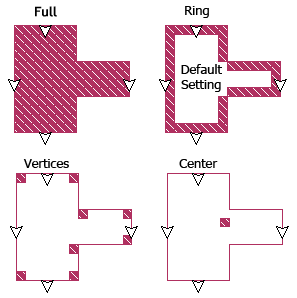
Ring
Ring meshing is the default meshing for new Via Tech Layers and is the recommended meshing for modeling most solid and hollow vias at DC and RF. The via polygon is modeled as a one cell wide wall of via subsections and is hollow in the middle, containing no metal. This meshing adequately models solid vias at RF because most of the current travels along the perimeter of the via.
Vertices
Vertices meshing models the via by placing a single cell via subsection at each vertex of the via polygon. Notice that if you use this model, the current may need to travel a longer path (i.e., longer than the real circuit) before it reaches a via subsection.
Center
A single cell wide via subsection is placed in the center of the via polygon. Note that if you use this model, the current may need to travel a longer path (i.e., longer than the real circuit) before it reaches the via. Therefore, you should use this option when you are not concerned about the path length.
Full
Full meshing models the via as solid metal. The interior of the via is filled with via subsections, extending the length of the via. This type of meshing is the most costly in terms of processing time and memory. This model should only be used if the via you are modeling is actually solid and you require a higher level of accuracy than that provided by Ring meshing.
Bar
This meshing identifies the via as being a Bar via. Bar vias are vias whose length is significantly longer than their width. This usually implies that they carry significant horizontal current. Since via subsections only carry vertical current, the decrease in loss is modeled by modifying the loss of the planar polygons to which they connect.
Your circuit may contain multiple adjacent bar vias as shown in the picture below.
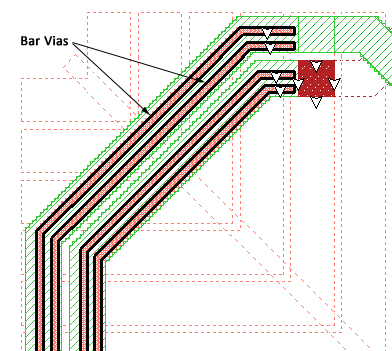
During the analysis, multiple adjacent bar vias are merged into one wider via to save memory and processing time. The illustration below shows some examples of Bar via groups.
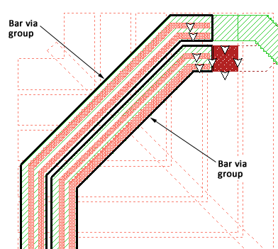
When the bar vias are grouped and simplified by the EM solver, they are meshed using Vertices mesh. Since Bar vias are only identified in the project editor, the polygon fill pattern for the Bar via polygon is simplified. The actual subsections analyzed by the EM solver is calculated during the analysis.
Bar vias are identified in the project editor by assigning Bar meshing to a Via Tech Layer or by overriding the Via Tech Layer for one or more via polygons. This assignment may also be done automatically, when using a translator or interface to Sonnet (See Bar Via Group Simplification).
Advanced
You may edit the advanced properties of a via Tech Layer by clicking the Advanced button in the Meshing section of the Tech Layer Properties dialog box. Each option is described below.
Enable Meshing
Be default, the EM solver meshes all polygons in a Tech Layer. If the Enable Meshing checkbox is unselected, the EM solver will not create subsections for the polygons. The purpose of disabling the meshing is till allow you to temporarily hide part of your circuit from the EM solver.
Via Pads
Selecting the Via pads checkbox adds planar metal to the top and bottom of the via that is the same size and shape as the via polygon. The pad is modeled using planar metal with loss equivalent to the loss of the via metal being used for the via polygon.
Vias Stop at Metal Polygons
Normally vias extend from the specified beginning metal level to the specified ending metal level. However, if Vias stop at metal polygons is enabled, then a via will terminate if its path, contacts planar metal.
In the illustration below, the Tech Layer, "Via1" begins at level 0 and ends at level 2. The planar polygon at level 1 intersects the via. When Vias stop at metal polygons is not selected, as shown in the first picture, the via continues to level 2. But if Vias stop at metal polygons is selected, the via stops at level 1.
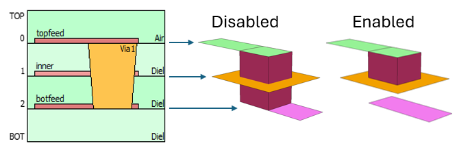
Note that the via is depicted in both the 2D and 3D view as the actual metal which will be analyzed. However, the associated Via Technology Layer still appears unchanged in the Stackup Manager because other vias associated with the Via Technology Layer may still extend the fully defined length. Only polygons which completely cover the cross-sectional area of the via are guaranteed to affect the height of the via.
The examples inductor_mim_cap and mmic_stage use this feature and may be obtained using the Example Browser.
Metal Model
The Metal Model determines the cross-sectional area used to compute the loss of a via. See Conductor Properties for information on specifying via loss.
Enabling Solid or using a Wall Thickness does not affect the meshing. The meshing is set Meshing.
The following sections explain how the Metal Model affects the area used for the loss computations.
Volume
The Volume via Metal Model allows you to specify your vias as solid via or hollow vias. For hollow vias, you unselect the Solid checkbox and specify a Wall Thickness.
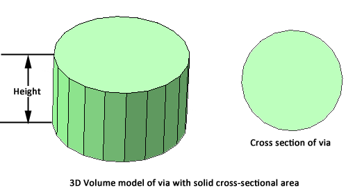
Solid
If your vias are solid, you should select the Solid checkbox. The complete area of the via polygon is used for the loss calculations. In the picture below, the cross-sectional area is the area of the circle.
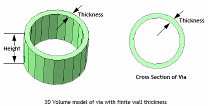
Wall Thickness
If your vias are hollow, you should unselect the Solid checkbox and enter the wall thickness of your vias. The wall thickness and the shape of each via polygon are used to determine the cross-sectional area used for the loss calculations. In the illustration below, a 3D view of the via is shown on the left, with the cross-sectional area shown on the right.
Array
When your circuit contains an array of many small individual vias, the large number of vias in the array may drive the memory and analysis time requirements beyond what is practical to analyze. This often requires that you simplify the via arrays before performing your EM simulation. This simplification can be performed automatically by one of Sonnet's translators or interfaces (see Via Array Simplification). Upon simplification, groups of many small vias are simplified into fewer larger vias. You may also simplify your via arrays manually by replacing the many small vias with a larger via polygon and setting the Metal Model to Array.
The cross-sectional area used to compute the loss is computed using a Fill Factor or Density which is based on the original via array.
Fill Factor: The Fill Factor is a percentage indicating how much of the cross-sectional area of the original via array is filled with metal. The Fill Factor is calculated by summing the areas of all the individual vias in the array and dividing by the total area of the simplified via. An example of a 5 by 10 array is shown below. The top picture shows the original array of 50 via contacts. Each via has a cross-section of 20 microns by 20 microns, or 400 square microns. Since there are 50 vias, the total cross-sectional area of the vias is 50 X 400 = 20,000 square microns. The area of the simplified via is 140 X 290 = 40,600 square microns. Thus, the Fill Factor works out to be 20,000/40,600 = 49.3%. The simplified via is shown on the bottom.
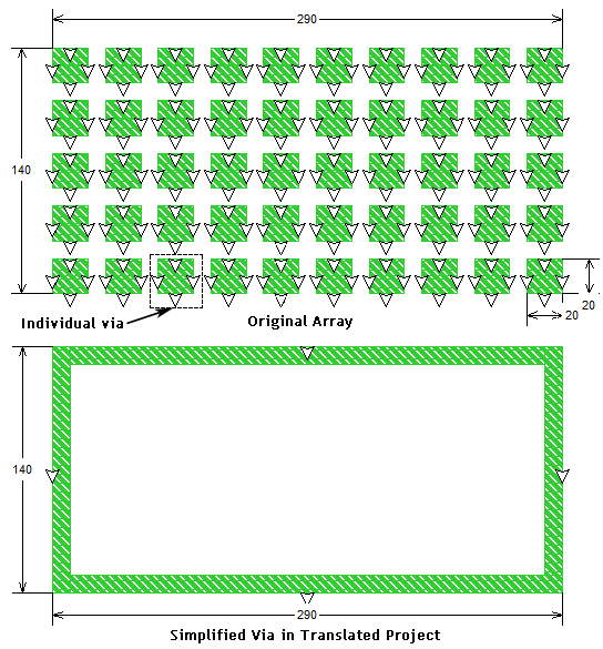
Density: The Density value is only used if the via's conductor material uses Resistance Per Via to specify its loss properties. The Density is the number of vias per square micron. The area is calculated based on the simplified via's area. In the example above, the Density would be 50/40,600 = 0.0012315.
The Array Via Metal Model is incompatible with Bar Meshing and the Surface Impedance Loss Type. The EM Solver will issue an error message and stop if either of these combinations is detected.
Edge Vias
Edge Vias are vias that are attached to the edge of a metal polygon. Edge Vias provide a quick, convenient way to add a one-cell wide via which extends for the length of the polygon edge. Edge Vias use the same conductor properties as the polygon to which they are attached. The example shown below uses an Edge Via to connect two polygons on adjacent levels.