Tech Layers Overview
A Tech Layer allows you to define a group of polygons with common properties including the metal level on which they are placed. This enables you to more easily control a large group of polygons and make changes to them as efficiently as possible. Tech Layers provide uses and advantages similar to drawing layers in CAD and EDA programs.
There are five types of Tech Layers:
- Planar: Horizontal metal. Usually the majority of your circuit is composed of planar metal.
- Via: Vertical metal, usually used to connect planar metal polygons located on different metal levels.
- Brick: A solid volume of localized dielectric material embedded within a dielectric layer.
- Derived: A Tech Layer that is derived from a rule involving one or more Tech Layers.
Click any of the links above to learn more about each specific Tech Layer.
Creating Tech Layers
Tech Layers may be created using any of the following methods:
- You may use Circuit > Settings > Tech Layers and click the appropriate Add button.
- You may right-click on a dielectric layer in the Stackup Manager and select the appropriate Add command from the list.
- If you insert a polygon on a level that does not already contain a Tech Layer of the type of polygon you are adding, you will be prompted to enter the properties of a new Tech Layer and one will be created.
- When you use a Sonnet Interface or one of Sonnet's import wizards, Tech Layers are automatically generated.
Deleting Tech Layers
Use one of the following methods to delete a Tech Layer:
- Right-click on the desired Tech Layer in the Stackup Manager, then select Delete Tech Layer from the pop-up menu which appears.
- Select Circuit > Settings > [Tech Layers] and select one or more Tech Layers you wish to delete. Then click the Delete button.
Moving Tech Layers
To move a Planar or Brick Tech Layer to a different level, follow these steps:
Double-click the desired Tech Layer in the Stackup Manager.
The Tech Layer Editor dialog box appears on your display. Alternatively, click Circuit > Settings > [Tech Layers], select a Tech Layer, and click the Edit button. You may also double-click a Tech Layer.
Select the metal level to which you wish to move the selected Tech Layer from the Level drop list.
Click the OK button to close the dialog box and apply the changes.
The Stackup Manager is updated and displays the Tech Layer in its new location. All polygons associated with the Tech Layer are moved to the new level maintaining the same x,y location.
A similar procedure may be used to change the Begin and End levels of a Via Tech Layer.
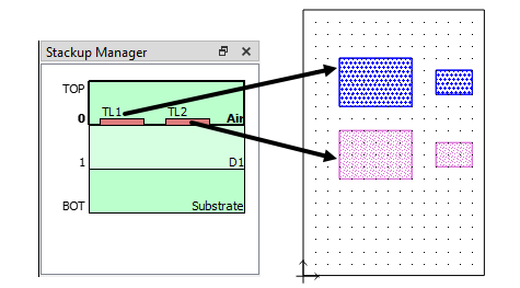
Multiple Tech Layers on a Metal Level
You may create more than one Tech Layer on any given metal level. For example, as pictured below, Level 0 of this circuit contains two Planar Tech Layers: TL1 and TL2. This may be useful if, for example, you wanted some polygons to use a different meshing from other polygons on the same level.
Overlapping Polygons
If two or more polygons on the same level overlap, and those polygons have different properties, an algorithm is used to determine the properties of the overlapping area. The algorithm uses a Tech Layer property called "Precedence". The following rules are used to resolve overlapping polygons on the same level:
- In the overlapping area, the Precedence value of each Tech Layer is compared. The properties of the Tech Layer with the highest Precedence is used.
- If there is more than one Tech Layer with the highest Precedence, then the loss of the overlapping area is based on a parallel combination of the Tech Layers.
- Only Tech Layers of the same type and with identical levels are compared.
The default Precedence value of a Tech Layer is 0. If all Tech Layers have a Precedence of 0, the Precedence value is not shown in the Tech Layer Properties dialog box unless the preference, Always Show Precedence Controls, is enabled (see Project Editor Preferences).
Inherit vs. Override
By default, an object inherits its properties from its parent. For example, polygons inherit their properties from the Tech Layer to which they are assigned. There are two types of inheritances which may be overridden, as explained below.
Polygon Overriding a Tech Layer
By default, polygons inherit their properties from the Tech Layer to which they are assigned. In general, if you need a set of polygons to have different properties than their Tech Layer, you should create a new Tech Layer for those polygons. However, sometimes it is more convenient to use the same Tech Layer for both sets of polygons. For such cases, you may wish to override the Tech Layer properties. For example, you may wish to set the meshing properties of one polygon to be different from the rest of the polygons of a Tech Layer. To override the properties of one or more polygons, follow these steps:
Select the polygon(s) you wish to change.
Edit the properties of the selected polygon(s).
Select either Planar Properties, Via Properties, or Brick Properties, from the Object menu or the right-click menu.
In the Polygon Properties dialog box, select the Override radio button.
The override section of the dialog box is now available for editing.
Make any changes to the properties you wish to override.
After making a change to a property, the inheritance icon for the changed property changes from an inherit icon to a override icon.
| Icon | Meaning |
| Inherit: This icon indicates that the property is inherited from its Tech Layer (default). | |
| Override: Indicates that one or more properties are overridden from their Tech Layer. | |
| Mixed inheritance: This icon is displayed when multiple polygons have been selected, and some polygons inherit their properties from the Tech Layer and some are overridden. |
You may wish to change the color or pattern of the polygon to help you remember that the polygon is overriding the Tech Layer properties.
Click OK to save your changes.
The number of overridden polygons associated with a Tech Layer may be seen by selecting Circuit > Settings > [Tech Layers]. The # Overrides column displays the number of polygons which are set to override their Tech Layer properties.
Tech Layer Overriding a Technology File
If your project is linked to a Technology File, Tech Layers inherit their properties from the Technology File. However, under rare circumstances, you may wish to change the properties of a Tech Layer without changing the Technology File. To override the properties of one or more Tech Layers, follow these steps:
Open the Tech Layers Properties dialog box for the Tech Layer(s) you wish to edit.
You may click Circuit > Settings > [Tech Layers], and select one or more Tech Layers, followed by clicking the Edit button. Alternatively, select one or more Tech Layers from the Stackup Manager, then right-click on one of the selected Tech Layers and select Tech Layer Properties from the pop-up menu.
In the Tech Layer Properties dialog box, select the Override radio button.
The override section of the dialog box is now available for editing.
Make any changes to the properties you wish to override.
After making a change to a property, the inheritance icon for the changed property changes from an inherit icon to a override icon. See the table of icons in Polygon Overriding a Tech Layer.
Click OK to save your changes.
Tech Layer Mapping
Tech Layer Mapping may be viewed or edited by clicking the Edit Mapping button in the Tech Layer Properties dialog box. When a layout is imported into Sonnet from another design environment, mapping information is automatically added to the Tech Layer. This provides continuity between the two environments. In addition, if you export the Sonnet layout to the original or a different design environment, the layers are re-mapped using this information. If you hover your cursor over a field in the dialog box, a tooltip pops up with a brief description of each field.