Planar Tech Layers
Planar Tech Layers group planar metal polygons that share the same properties, including the level on which they reside. Any change made to the properties of a Planar Tech Layer is immediately applied to all the polygons assigned to that Tech Layer (see Inherit vs. Override for an exception).
To add a Planar Tech Layer, select Circuit > Settings > [Tech Layers], select the Tech Layers tab and click the Add Planar button. The Tech Layers Properties dialog box will launch. Alternatively, if you wish to edit an existing Planer Tech Layer, select select the Tech Layer you wish to edit, and click the Edit button. You may also edit a Tech Layer using the Stackup Manager.
The Tech Layer Properties dialog box allows you to specify the following information:
Name: The name must be unique, is case sensitive, and cannot contain any of the following characters:
Level: The Level field corresponds to the Sonnet metal level to which the Planar Tech Layer is assigned. You may assign multiple Tech Layers to a single metal level including multiple Tech Layers of the same type.
Conductor: The Conductor section allows you to specify the material properties of the Tech Layer. You may use an existing conductor material or define a new one.
Meshing: The Meshing section allows you to specify the type of subsections used and the subsectioning controls. See Subsectioning for more details.
Metal Model: The Metal Model section determines how the EM solver models the thickness of the metal. See the Metal Models section below for more details.
Roughness: The Roughness section allows you to specify any surface roughness. See Roughness below for details. By default, conductor surfaces are assumed to be perfectly smooth.
Color/Pattern: The color and pattern of the polygon is used to help you identify the Tech Layer in the Project Editor.
Mapping: When a layout is imported into Sonnet from another design environment, mapping information is automatically added to the Tech Layer. This provides continuity between the two environments. In addition, if you export the Sonnet layout to the original or a different design environment, the layers are re-mapped using this information. If you hover your cursor over a field in the dialog box, a tooltip pops up with a brief description of each field.
Metal Models
The Metal Model section of the Tech Layer Properties dialog box allows you to choose how to model the metal thickness (i.e., the z-direction). Select the model from the drop-down list and specify the metal thickness in the text entry box. You may click the Advanced button to specify advanced options for the chosen model. Each model is explained in detail below.
Thin Metal Model
By default, a planar conductor polygon uses the Thin Metal model. A Thin Metal polygon is modeled as a 2D sheet of zero thickness as shown below.
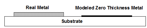
Thin Metal is the default and most commonly used metal model because it is the most efficient. It may be used to model electrically thin conductors (low frequency), electrically thick conductors (high frequency), and the transition between electrically thin and electrically thick. See references [7] and [8] for a detailed description of the theory and equations used by Sonnet to calculate loss.
For the Thin Metal model, metal thickness is used only in calculating loss. The metal is still modeled as a zero-thickness 2D sheet, regardless of the thickness specified.
Current Ratio
The current ratio is an advanced parameter used by the Thin Metal model. At high frequencies, current flows in a thin skin around the edge of the metal. Since there are no sides in a zero thickness model; the current which flows on the sides is ignored. The Current Ratio is defined as the ratio of the current flowing on the top of the metal to the current flowing on the bottom of the metal at very high frequencies, where the thickness is much greater than a skin depth. The current ratio may be set to any non-negative real number.
The default Current Ratio is 0.5. This is a compromise value based on using planar metal in a wide variety of transmission line structures. You can adjust this value as needed for your particular application. To help you decide on a suitable value, refer to the table below which gives recommended values for the current ratio for various applications.
| Application | Recommended Current Ratio |
| Symmetrical Stripline | 1.0 |
| Coplanar waveguide (CPW) signal lines | 0.5 |
| Microstrip signal lines | 0.5 |
| Polygon ground planes below the signal line | ≥1000 |
| Polygon ground planes above the signal line | 0.0 |
The table above shows that the current ratio depends on the type of circuit being simulated.
- For symmetrical stripline, at very high frequency, the current is equally split between the top and bottom surfaces, resulting in a current ratio of 1.0.
- For microstrip and CPW circuits, the current is usually unequally distributed. The range could be anywhere between 0.0 to 1.0, but in our tests, we have found that the majority of microstrip and CPW traces have a current ratio between 0.4 and 0.6.
- For ground planes at high frequencies, most of the current flows on the surface nearest the signal lines, so you should enter a small current ratio (e.g., 0.0) when the signal line is below the ground plane and enter a large current ratio (e.g., ≥ 1000) for when the signal line is above the ground plane.
Thick Metal Model
The Thick Metal model is used to model physically thick planar conductors. This model is more accurate in modeling metal thickness, but uses more computer resources.
The Thick Metal model approximates a thick conductor by modeling the conductor with two or more infinitely thin sheets of metal that are electrically connected along the edges with vias. The number of sheets used by the model is an input parameter. The default number of sheets is two, with the upper sheet placed at the top surface of the conductor, and the lower sheet placed at the bottom surface of the conductor. A 3D illustration of how a thick conductor is meshed when the Thick Metal model is used with two sheets is shown below:
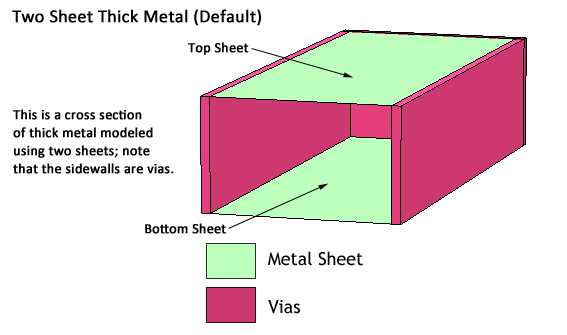
It is important to note that the via walls along the edges of the conductor carry only z-directed current. XY-directed current will only flow in the infinitely thin planar sheets. For the two-sheet Thick Metal model, this means that the XY-directed current flows only on the upper and lower surfaces of the conductor.
Number of Sheets
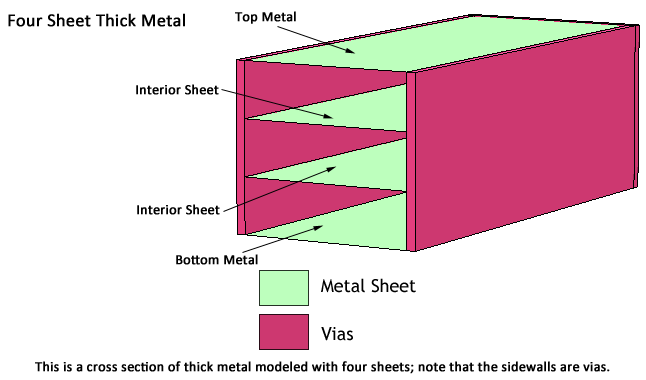
For most cases, using the default of two sheets provides a sufficiently accurate solution. However, for tightly coupled lines, where the gap between the lines is less than the metal thickness, coupling between the lines may be underestimated if only 2 sheets are used. Under this circumstance, increasing the number of sheets used will improve the accuracy of the coupling calculations. Please note, however that increasing the number of sheets used will also result in higher memory requirements and longer processing time for the simulation. A 3D illustration of a how a thick conductor is meshed when the Thick Metal model is used with four sheets is shown below.
Z-Mesh Method
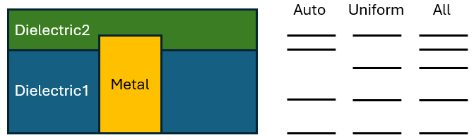
When more than two sheets are specified, the additional sheets are placed equidistant from each other, unless the conductor is thicker than the dielectric in which it resides. When this occurs, it is more efficient to place the additional sheets on boundaries between the two dielectric layers instead of placing the sheets equidistant from one another. However, under some circumstances, such as if the resulting sheets are extremely close to each other, this method could reduce accuracy. If you wish to control how the additional sheets are placed, choose one of the following options.
- Auto placement: The conductor is modeled with the number of specified sheets. When more than two sheets are specified and there are no dielectric boundaries, the additional sheets are placed equidistant from each other. If there are dielectric boundaries, the additional sheets are first placed at any dielectric boundaries within the metal thickness. Any additional sheets are kept as far away as possible from other sheets. This is the default setting.
- Uniform placement: The conductor is modeled with the number of specified sheets. When more than two sheets are specified, the additional sheets are placed equidistant from each other even if there are dielectric boundaries. This method may be less efficient than the Auto placement method but guarantees the sheets are uniformly distributed.
- All boundaries: The conductor is modeled with a number of sheets equal to the number specified plus additional sheets are placed at all dielectric boundaries within the metal thickness. This may result in more sheets than specified. This method was used by Sonnet release 18 and earlier. Therefore, if you import an old project into the present Sonnet release, this setting will be used.
The following picture illustrates the different methods when the number of sheets is set to 4. The left side shows a side view of metal that is thicker than Dielectric1. On the right, black lines indicate the location of the sheets for each method.
TrueVolume Model
The TrueVolume model divides the volume of a thick conductor into rectangular metal cubes, and then uses Sonnet's volume subsections to model those cubes. These volume subsections account for the full 3D geometry of a subsection in all coupling calculations. Therefore, the physical thickness of the metal conductor is inherently accounted for with the use of volume subsections.
Z-Mesh Method
The vertical divisions or Z-Meshing of the thick conductor, are optimized to automatically provide maximum accuracy in terms of loss and capacitive coupling. This is important as the distribution of current on and within a thick conductor is a function of the conductor properties, frequency, and the proximity of the conductor to other nearby conductors. Sonnet provides two options to control this Z-meshing:
• Single layer surface
• Double layer surface
The Single layer surface method is the default method, and it has the minimum requirements in terms of computer resources. Shown below is a cross-section of a TrueVolume conductor using the Single layer surface Z-Mesh method:
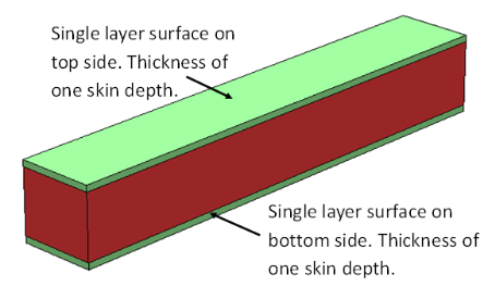
For this method , the TrueVolume conductor is divided into three layers:
- A top surface layer that is one skin-depth thick.
- A middle Layer
- A bottom surface layer that is one skin-depth thick.
The Double layer surface method is the preferred method when there is strong capacitive coupling between the TrueVolume conductor and other nearby conductors. Shown below is a cross-section of a TrueVolume conductor using the Double layer surface Z-mesh method:
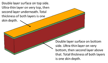
For this method, the True Volume conductor is divided into five layers:
- An ultra-thin outer layer on the top side. Required for accurate capacitive coupling calculations.
- An internal layer near the top side. The sum of layers 1 and 2 is one skin depth thick
- A middle layer.
- An internal layer near the bottom side. The sum of layers 4 and 5 is one skin depth thick.
- An ultra-thin out layer on bottom side. Required for accurate capacitive coupling calculations.
Roughness
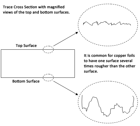
Many circuit manufacturing processes produce planar metal with rough surfaces. Depending on how the metal is formed, one or both of the trace metal surfaces could be relatively rough. At frequencies where the skin depth is comparable or smaller than the surface roughness dimension, the current flow is forced into the surface roughness region and this introduces excess resistance and excess inductance in your traces. This in turn increases the insertion loss and insertion phase of your transmission lines. Sonnet uses the results of an extensive study of surface roughness effects in printed circuit board conductors. See references [9] and [10] for a detailed description.
The Rough Metal section of the Tech Layer Properties dialog box allows you to specify the surface roughness of your metal traces. You must first obtain the top and bottom surface roughness in RMS microns for the metal. Often circuit material suppliers provide this information directly or you can ask the manufacturing group producing your physical parts.
Surface roughness can also exist on ground plane metal. If you are using an Analysis Box cover to represent a ground plane, you can define a surface roughness to the top and/or bottom box cover. See Covers Tab for details.
Care should be taken when using the results in a time domain simulation, as the Rough Metal results are not guaranteed to be causal.