Tutorial: Use Project Editor for Layout
This part of the tutorial teaches how to use the Project Editor to add the spiral inductor layout to the project file, part1_settings.sonx, which you created in the first part of this tutorial. The part1_settings.sonx file contains all the settings, such as units, box settings, cell size, material properties, dielectric layers, Tech Layers, frequencies, and EM options. This file is also available in the Getting Started Tutorial example which you may obtain using the Example Browser. Click the triangle below to expand the instructions for obtaining the example file.
Obtaining the Example FileObtaining the Example File
To obtain the example file, follow these instructions.
Select Help > Browse Examples from any Sonnet tab.
The Example Browser opens.
Find the Getting Started Tutorial and select it.
You may use the search box or scroll down until you see the Getting Started Tutorial example.
Click the Save button at the bottom of the Example Browser window.
A Save Example window opens with a list of files that will be saved.
Enter or browse for the folder where you wish to place the example files.
Choose a location you can remember.
Click the Save button.
The example files are saved to the specified folder.
Click the Close button.
The Example Browser closes.
If you have not done so already, open the file, part1_geometry.sonx in the Sonnet Project Editor.
Add Spiral Shape
In this section, you will add the spiral portion of the geometry to the Spiral Tech Layer.
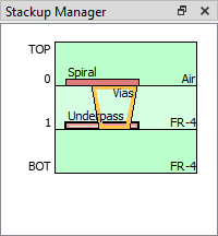
Select the Spiral Tech Layer in the Stackup Manager.
The active level becomes level 0 and the Spiral Tech Layer symbol is selected as shown below:
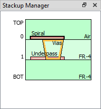
When you place the spiral geometry, it will be placed on the Spiral Tech Layer by default.
Select Insert > Planar Rectangular Spiral.
The Rectangular Spiral Properties dialog box opens.
The Insert menu contains a list of common shapes that can be added to your project. See Adding a Standard Geometry for details.
Enter the properties of the spiral using the table shown below.
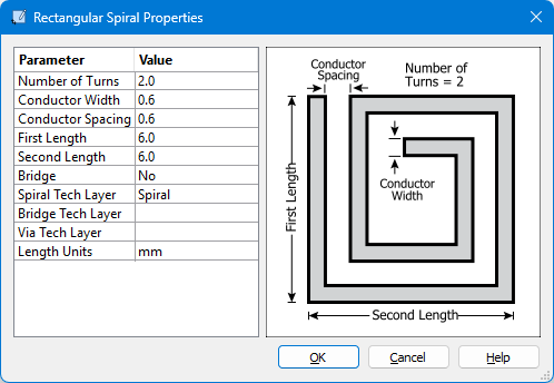
You will be adding a two-turn rectangular spiral with a width and spacing of 0.6 mm and a length and width of 6.0 mm. Also notice that the Bridge is set to No because you will be adding a bridge manually.
Click OK.
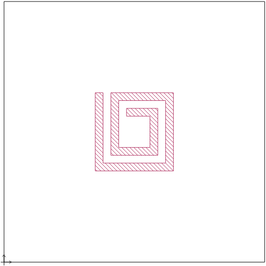
The dialog box closes and an outline of the spiral is displayed which moves with your cursor. The outline represents the location where the spiral shape will be placed when you click your mouse.
Click near the center of the box to place the spiral shape.
The spiral shape is added to the Spiral Tech Layer. Don't worry about the precise placement. In the next step, you will center the spiral shape in the box.
Center Spiral
It is usually a good idea to keep your circuit centered in the Analysis Box to reduce the coupling to the box walls.
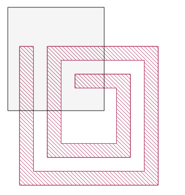
Click on the spiral polygon to select it.
The polygon is highlighted with a black outline to indicate that it is selected.
Select Object > Center > Both.
The spiral polygon is centered in the Analysis Box.
Select Select > None.
A polygon is unselected.
You may also click any blank area in your circuit to unselect all polygons.
Your project should look similar to the picture below:
Add Underpass
Next you will add a rectangular underpass to the Underpass Tech Layer. But first, you will zoom into the area to make it easier to place the underpass.
Select View > Zoom to enter Zoom mode.
Your cursor changes to the zoom cursor to indicate you are in Zoom mode.
You may also enter Zoom mode by pressing the space bar on your keyboard, or clicking the Zoom button  on the toolbar.
Using your mouse, drag a region surrounding the top left portion of the spiral as shown below:
The zoom area is indicated in the first picture below, and the second picture shows the view after zooming.

After zooming, you should be able to see the cell grid (black dots). Make sure you can see the open end of inner turn of the spiral.
You can also use the Zoom In button  and Zoom Out button
  on the toolbar and/or your mouse's middle scroll wheel to refine your zoom area.
Select the Underpass Tech Layer in the Stackup Manager.
The active level becomes level 1 and the Underpass Tech Layer symbol is selected as shown below:
The spiral polygon is shown as a dashed line to indicate that it is not on the active level. When you place the spiral geometry, it will be placed on the Underpass Tech Layer by default.
Select Insert > Planar > Planar Rectangle.
The Rectangle Properties dialog box opens.
Enter the 0.6 and 2.9 for the Width and Height of the underpass.
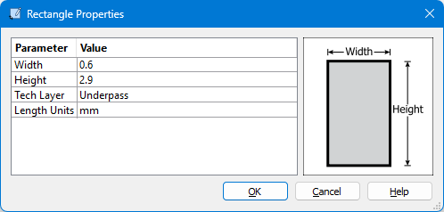
You will be adding a rectangle with a width of 0.6 mm and a height of 2.9 mm. Also notice that the Tech Layer is set to the Underpass Tech Layer.
Click OK.
The dialog box closes and an outline of the rectangle is displayed which moves with your cursor. The outline represents the location where the rectangle will be placed when you click your mouse.
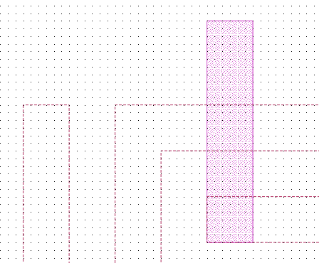
Place the rectangle at the location shown below.
Add Vias
The next step is to add circular vias that will connect the spiral polygon to the underpass polygon.
Select the Vias Tech Layer in the Stackup Manager.
The active level becomes level 0 and the Vias Tech Layer symbol is selected as shown below: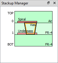
The Spiral and Underpass Tech Layer symbols are now filled, indicating that there is at least one polygon assigned to them. The Vias Tech Layer symbol is unfilled, indicating that there are no polygons assigned to the Vias Tech Layer.
Select Insert > Via > Circular Via.
The Circle Properties dialog box opens.
Enter "0.4" for the diameter of the circular via.
The properties dialog box should look similar to the image shown below:
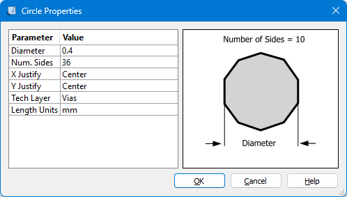
You will be adding a circular via with a diameter of 0.4 mm. Also notice that the Tech Layer is set to the Vias Tech Layer.
Click OK.
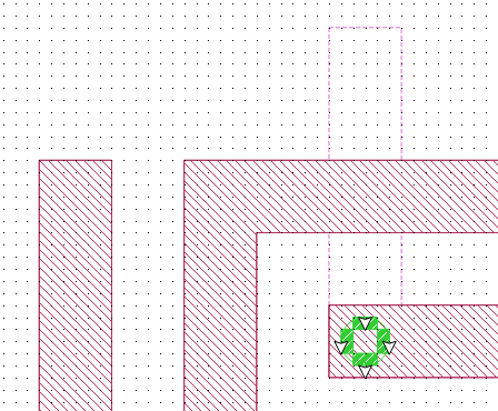
The dialog box closes and an outline of the circular via is displayed which moves with your cursor. The outline represents the location where the via will be placed when you click your mouse.
Place the first via at the location shown below.
You will now insert the second via using a slightly different method.
Click the Insert Circular Via button ![]() located in the Insert toolbar.
located in the Insert toolbar.
By default, the Insert toolbar is located on the right side of the Project Editor window. This toolbar button is always set to the last via inserted but may be changed by clicking the down-arrow next to the button label. In this case, the circular via is the last via inserted. Clicking this button is identical to selecting Insert > Via > Circular Via.
The Circle Properties dialog box is opened and the settings should be the same as the last time you inserted a circular via.
Click OK.
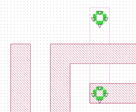
The dialog box closes and an outline of the circular via is displayed which moves with your cursor.
Place the second via at the location shown below.
Draw Via Pad
You will now draw a square via pad above the second via you just created.
Select the Spiral Tech Layer in the Stackup Manager.
The active level becomes level 0 and the Spiral Tech Layer symbol is selected as shown below:
Select Insert > Draw Rectangle.
Your cursor changes to the Draw Rectangle cursor, waiting for you to draw the pad.
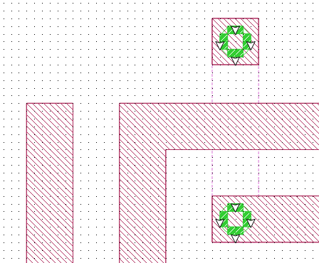
Click the top left corner of the underpass polygon and draw a 0.6 mm by 0.6 mm rectangle.
To create a rectangle, you click two opposite points to define the rectangle. The ΔX and ΔY values in the status bar show you the size of the resulting rectangle. The animation below shows the process.
When finished, your pad should look like the picture below.
Extend Length
You will now extend the outer length of the spiral to line up with the via pad.
Select Edit > Edit Points.
You may also use the Edit button ![]() in the Edit toolbar. Your cursor changes to indicate you are in Edit Points mode. This mode allows you to move or delete individual points or a group of points.
in the Edit toolbar. Your cursor changes to indicate you are in Edit Points mode. This mode allows you to move or delete individual points or a group of points.
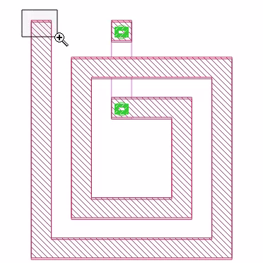
Use your mouse to lasso the two points as shown below.
Drag the points up by 1.1 mm so they are aligned with the top edge of the via pad.
Press the Esc key on your keyboard to exit Edit Points mode.
Your cursor changes back to the default Pointer Mode cursor.
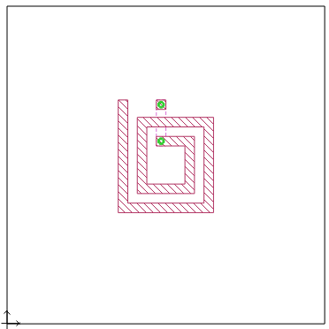
Select View > Full View.
This command resets the area displayed such that the circuit fills the available viewable area. Your circuit should look similar to the picture below:
You may also click the Full View toolbar button  instead of using the menu.
Recenter Circuit Metal
Since we added extra metal, the circuit is no longer precisely centered in the Analysis Box. Although this small difference is not critical, a few more tips can be learned by doing it.
Select Select > Select All.
All polygons in your circuit are selected.
You may also press Ctrl+A to select all polygons in your circuit.
Select Object > Center > Both.
The entire circuit is re-centered within the Analysis Box.
Select Select > Select None.
The selected polygons are unselected.
Snap to Grid
After the circuit was centered, the circuit is no longer snapped to the grid. This can be seen by zooming up on a portion of the circuit as described next.
Select View > Zoom.
Your cursor changes to the zoom cursor to indicate you are in zoom mode. The purpose of zooming up is to be able to see the cell grid.
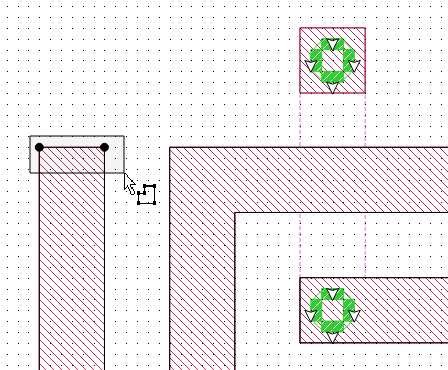
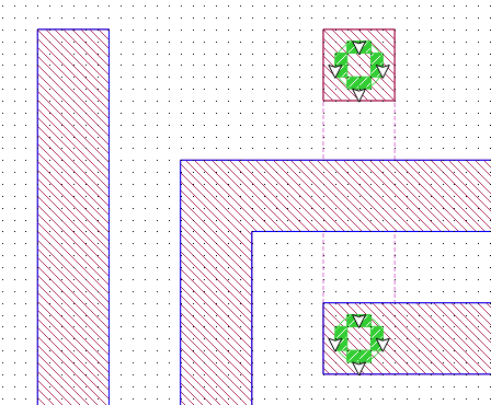
Using your mouse, drag a region surrounding the top left portion of your circuit.
The zoom area is indicated in the first picture below, and the second picture shows the view after zooming.
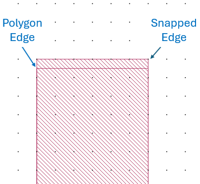
Notice two outlines are shown. The outline labeled "Polygon Edge" represents the exact geometry that you entered. The outline labeled "Snapped Edge" represents the actual subsections analyzed by the EM solver. The fill pattern always corresponds to the actual subsections analyzed by the EM solver. See The Analysis Grid for more details.
You may turn the snapped fill pattern on and off by selecting View > Polygon Fill > Snapped Fill and View > Polygon Fill > No Fill. See Polygon Fill for details and for additional viewing options.
It is not necessary to have all of your metal polygons snapped to the grid because the EM solver analyzes the snapped coordinates. However, it can sometimes be more visually appealing to have it snapped to grid. In the next steps, you will re-align the circuit to be snapped to the grid.
Select Select > Select All.
All polygons in your circuit are selected (even the ones you cannot see).
Only the polygon edges are highlighted with a thick black border. If a snapped edge is not coincident with a polygon edge, the snapped edge is not highlighted.
Select Object > Snap To.
The Snap To dialog box appears.
When you snap a circuit to the grid, you have a choice of snapping each vertex on all the selected polygon(s) to the grid or selecting a reference point to snap and having all other vertices maintain their position relative to that reference point. You will use the second mode.
Click the Select Reference Polygon Vertex button.
The dialog box temporarily disappears and your cursor changes.
Click the top left vertex of the spiral inductor.
The vertex is selected and the Snap To dialog box reappears. Notice that the the second mode, Preserve shape and spacing relative to the referenced point, is now selected.
Click OK.
The picture below shows that the previously unsnapped edge is now snapped.
When using the Preserve Shape mode, only the selected vertex is guaranteed to be snapped to the grid.
The entire circuit is now shifted by the same amount that the selected vertex was shifted.
Select View > Full View.
The area displayed is reset such that the circuit fills the available viewable area.
Select Select > Select None.
The selected polygons are unselected.
Save Your Progress
You have finished creating your layout, so it is a good idea to save your project now.
Select File > Save As and save the project as part2_geometry.sonx.
Next, you will finalize your project. Click the Next button below to continue.