Circuit Subdivision
Sonnet's Circuit Subdivision feature provides the capability to take a large circuit and split it into any number of smaller projects, then connect the results in a netlist project to produce EM results for the whole circuit. This method can significantly reduce the required processing time and memory necessary to analyze the circuit while still obtaining an accurate answer.
The use of Circuit Subdivision is demonstrated in the example bpfilter, which may be obtained using the Example Browser.
Circuit Subdivision in Sonnet allows you to insert Subdividers in your geometry using the Project Editor. These Subdividers create the sections from which the Subdivide command makes geometry subprojects. When you select the Subdivide command, the software creates a main netlist file and the geometry subprojects. The main netlist connects the subprojects so that the results for the netlist may be substituted for the results of the source project.
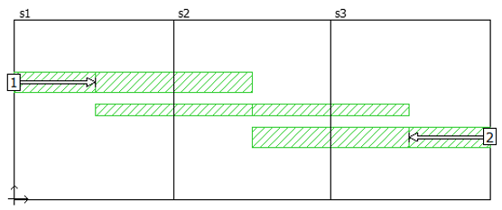
Source circuit with Subdividers
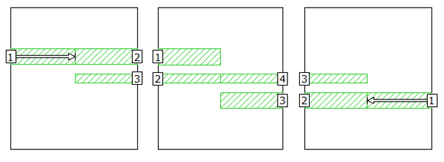
Generated subprojects
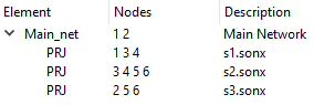
Main netlist
Procedure
Below is the list of steps required to perform Circuit Subdivision.
Create the baseline project
Choose the location of the Subdividers
Add Subdividers to mark where the circuit will be subdivided
Subdivide the circuit using the Subdivide command
Fine-tune the subprojects (optional)
Analyze the main netlist project
Each step is explained in detail in the following sections.
Create the Baseline Project
You start with the geometry project which you wish to subdivide. Since the geometry subprojects created by Circuit Subdivision inherit their properties from the source project, you should complete entering all the desired attributes for your circuit before performing the subdivide.
You should also be aware that if your main circuit contains any parameters or dimensions, they are not included in the subprojects. After the subprojects are created, you may enter parameters in any of the geometries. In fact, it is possible to run optimizations on the main netlist project using a parameter in one of the subprojects.
Choose Subdivider Locations
The next step is to choose the location of your Subdividers. This step often requires knowledge about your circuit because you need to avoid splitting the circuit at a location where there is coupling across the Subdivider.
The Subdividers should be placed between polygons which have negligible coupling. Places on the circuit where a high degree of coupling or rapidly varying currents are present should be kept within an individual subproject.
Long lengths of transmission lines in your circuit are usually good places to subdivide your circuit because there would be no coupling across the Subdivider. Long lengths of coupled transmission lines are also good places to place a Subdivider, provided your Subdivider is perpendicular to the flow of current. This point is illustrated below.
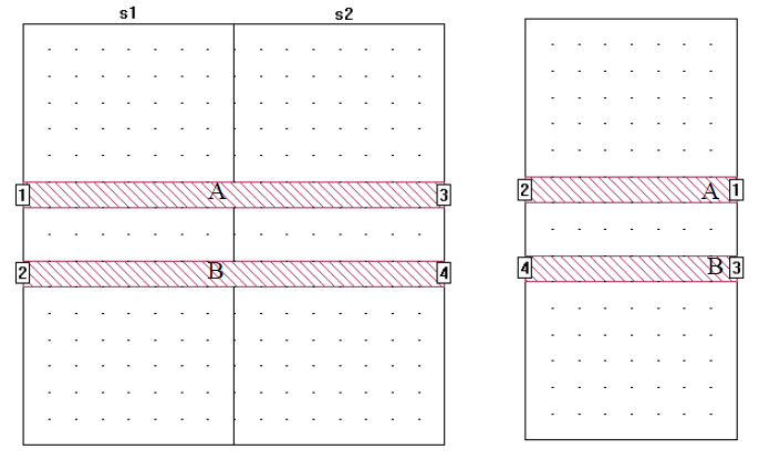
In the picture below, the left circuit consists of a coupled transmission line. This is too simple of a circuit to require subdivision, but is useful in demonstrating the principle. When subdivided, the circuit is split into two subprojects both of which would resemble the circuit shown on the right. Notice that the coupling between points A and B is maintained in the subdivided project.
Placing a Subdivider perpendicular to one or more transmission lines provides a good general guideline for Subdivider placement.
In addition, the following are restrictions for Subdivider placement:
- Subdividers must always be on a cell edge.
- Subdividers may not be colinear with polygon edges.
- Subdividers may not split a diagonal polygon edge.
- Subdividers may not split a port.
- Subdividers may not be below the line of symmetry.
- Subdividers may not split a polygon at a box wall.
The following sections contain a series of illustrations, each showing the good placement of a Subdivider and its counterpart showing a bad (and in some cases illegal) placement of a Subdivider.
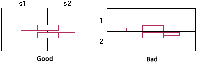
Example #1
The first example is a pair of coupled lines. When the coupled lines are split as shown on the left, very little loss of accuracy results because the coupling between the coupled lines is maintained. However, on the right, the Subdivider removes the coupling between the coupled lines.
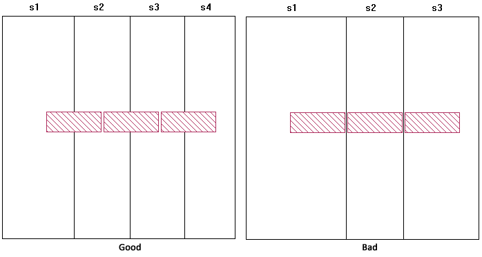
Example #2
This example shows how to split a series of resonators. In this type of structure, there is strong coupling at the gaps between adjacent resonators. The example on the left is good since the Subdividers do not prevent this inter-resonator coupling. The example on the right is bad since the resulting subprojects do not contain the inter-resonator coupling.
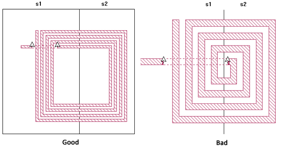
Example #3
This example shows a square spiral inductor. The example on the left is good since the location where the spiral inductor is divided is essentially a group of coupled transmission lines and the Subdivider is perpendicular to those lines. Here, the vertical lines on the left side of the spiral inductor are sufficiently far from the right side so that coupling is negligible. The example on the right is bad because the vertical lines and bends on the left side of the spiral inductor couple strongly with the lines on the right side.
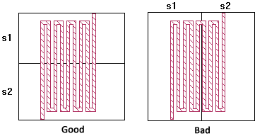
Example #4
The meander line on the left is split in such a way that Sonnet provides an accurate result since the bends on the top are far enough away from the bends on the bottom that coupling between them is negligible. The example on the right provides an inaccurate result because the coupling between two close transmission lines is eliminated by the Subdivider.
Example #5
The circuit shown below has coupled transmission lines on two different layers. Subdivision is valid for multi-layer structures as long as the coupling across the Subdivider is negligible.
Example #6
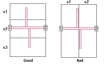
In the double stub circuit shown on the left, the Subdividers split the polygon perpendicular to the direction of current flow and far from any discontinuities. The circuit on the right however, shows the Subdivider splitting the bases of the two stubs which may be coupled.
Example #7
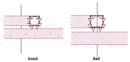
The Subdivider shown in the circuit on the right is bad since the circuit is split in the middle of a via between layers. In general, Subdividers should never be placed on top of vias or discontinuities. The Subdivider on the left is the correct placement.
Example #8
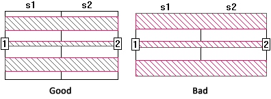
The Subdivider shown in the circuit on the right splits a polygon which touches the box wall. It is illegal to subdivide polygons grounded to the box walls since such polygons do not behave like transmission lines. Also, the new ports added during the subdivide would be shorted to the box-wall. The circuit on the left is correct since there is no contact between the top and bottom polygons with the top and bottom box wall.
Add Subdividers
The next step is to add Subdividers to mark where the circuit will be subdivided. Select Insert > Subdivider. If your circuit does not contain any subdividers, you will be asked to select the orientation of your Subdividers as explained in the next section.
Subdivider Orientation
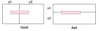
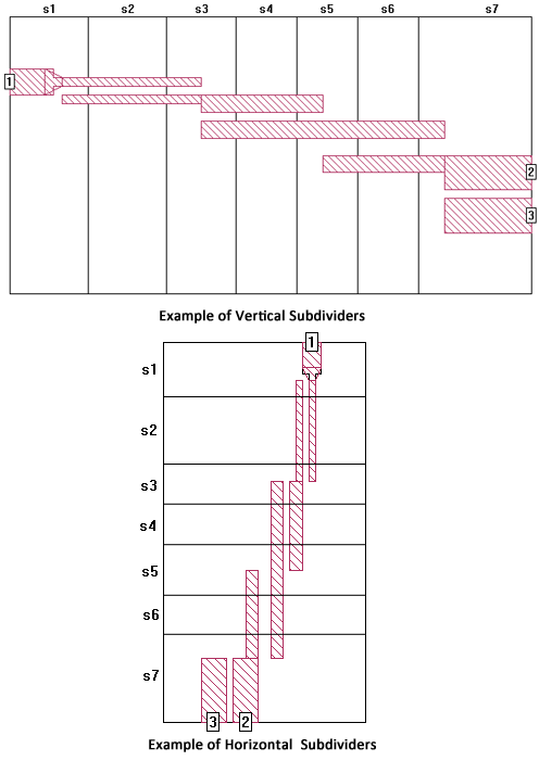
Subdividers may split the circuit on a horizontal axis or a vertical axis, but you may not mix orientation. Choosing the direction in which you split your circuit is dependent upon the structure of your circuit. Shown below is a typical circuit in which you would use the vertical orientation and another example in which you would use the horizontal orientation.
 You may use both orientations by using double subdivision. The first time you subdivide your main circuit you choose an orientation for your Subdividers. Then use Circuit Subdivision on the resulting geometry subprojects, this time using the opposite orientation for your Subdividers.
Placing the Subdivider
When you place a Subdivider in your circuit, a line representing the Subdivider appears on your circuit. The resultant sections of the circuit are automatically labeled. Subdivision sections are labeled from left to right, or top to bottom, depending upon orientation. These labels are always sequential and are non-editable.
Once a Subdivider has been added to your circuit, you may edit the Subdivider as you would any other object in your geometry. You may click and drag a Subdivider or use keyboard commands to move it. You may also control the selection and visibility of the Subdivider lines and labels using View > Options : [Select Filter] and View > Options : [Visibility] respectively.
Use the Subdivide command
The next step is to subdivide the circuit which will create the subprojects and main netlist project which connects the subprojects in a network equivalent to the circuit as a whole. Ports and feedlines with reference planes are added to the subprojects to allow the subprojects to be connected together.
You subdivide the circuit by selecting Circuit > Subdivide Circuit. A dialog box appears, allowing you to change the names of the projects that will be automatically created by the software. In addition, you may change the length of feedlines which are added to the subdivided projects. Feedlines should be added when discontinuities contained in sections of your source circuit need to be moved away from the box wall to prevent interaction between the box walls and the discontinuity. The use of feedlines are optional; if you choose to add a feedline, you may use the suggested length calculated by the software or input your own value. By default, the software creates feedlines using the suggested length.
Fine-tune the Subprojects (optional)
Each of the geometry subprojects uses the properties of the original circuit. In some cases, you may wish to change these properties to improve accuracy or analysis times. The most common property to change is the cell size since some subprojects may contain small geometries requiring a small cell size and others may contain large geometries which would allow a larger cell size.
You may also wish to add parameters to your subprojects. If you add parameters to a subproject in a netlist, the parameters are not automatically displayed in the main netlist. You must re-open the main netlist it to display the parameters and make them available for editing.
Analyze the Main Netlist Project
To obtain results for the subdivided circuit, analyze the main netlist project. Each subproject will be automatically analyzed by the EM solver. If properly subdivided, the results of the netlist analysis should provide an accurate solution for your circuit using fewer resources than the original circuit.