Introduction
This tutorial provides you with an overview of the Sonnet products and how they are used together. We walk you through a simple example from entering the circuit in the graphical project editor, to viewing your data in the response viewer, our plotting tool and in our current density viewer. The tutorial will also cover design issues which need to be considered in the project editor.
There are also tutorials on different Sonnet features in the Sonnet User’s Guide as well as tutorials on the use of the translators and interfaces in each of their manuals.
This tutorial is designed to give you a broad overview of the Sonnet suite, while demonstrating how to create a geometry project and run an analysis. The following topics are covered:
- An overview of the Sonnet Design Suite
- How to access Help
- The Sonnet session window
- Creating a circuit geometry project in the project editor
- Creating a New Project
- Units
- Box and Cell Size
- Box Cover Metals
- Dielectric Layers
- Technology Layers
- Drawing the Circuit
- Em, the analysis engine.
- Plotting data in the response viewer.
- Viewing current density data.
The Sonnet Design Suite
The suite of Sonnet analysis tools is shown below. Using these tools, Sonnet provides an open environment to many other design and layout programs.
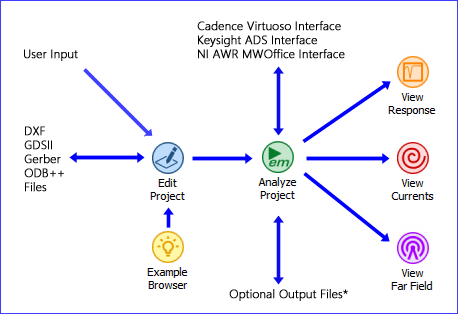
*See Optional Output Files for more details.
Sonnet provides the ability to import files from other interfaces and formats. There are specific tutorials for each of the translators and interfaces, but even if you plan on importing all your circuits, we suggest doing this tutorial to acquaint yourself with the Sonnet environment.
Help Resources
You may access information on running your software using the following methods:
- The documentation for Sonnet is available by selecting Help - Sonnet Help from any tab.
- You may get information for a specific tab type by selecting Help - Help on this tab from the main menu of any tab.
- You may get information on any Sonnet dialog box by clicking on the Help button in the dialog box.
- If you cannot find the answer to your question, you may contact Sonnet Technical Support by phone, email, or by filling out an online form. Please see our Ask a Question page for contact information.
Session Window
When you invoke Sonnet software, you start a session. A Sonnet session defines what Sonnet software is presently running, including what modules (tabs) are open, and how the interface tabs are configured. You may only have one session running at a time but there is no limit to how many windows and tabs are created, nor how many projects are opened. The session manager which appears in every type of Sonnet tab, including the default session tab, allows you to keep track of every tab and project that is open in the present session.
The session information is automatically saved and used the next time you run Sonnet. You can also manually save and load sessions using a session file (.sesn) if you wish. If you do not wish to open the last session when invoking Sonnet, see the Edit Preferences dialog box in the session tab.
A session file stores the following information:
- What tabs are open.
- What projects are open and in which tabs.
- The window configurations of the tabs including placement of panels and toolbars.
- Contents of the session manager.
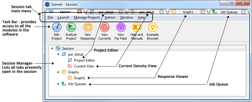
The Project Editor
The project editor provides you with a graphical interface which allows you to specify all the necessary information concerning the circuit you wish to analyze with the electromagnetic simulator, em.
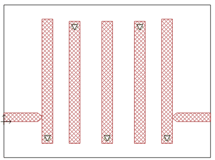
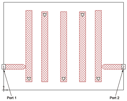
The example circuit, “idig_fil5.son”, shown below, is a 5-section, microstrip interdigital bandpass filter, with direct-tapped resonators, and center frequency of 5 GHz. Each resonator element is approximately one quarter-wavelength long at the center frequency and one end connects to the box bottom cover (ground) with a via.
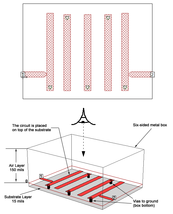
In the illustration above, the top is a two-dimensional view from the top looking directly down on the substrate. This is the view shown in the Edit tab. The bottom of the illustration shows a three-dimensional view of the circuit in the six-sided metal box modeled in the project editor, as displayed in the 3D tab.
Creating a New Project
For this tutorial, you will start with a new blank project and enter the example circuit shown above. A geometry project contains a geometry circuit whose properties are entered by the user or provided by translating a file to the Sonnet environment. The geometry project contains the layout and material properties of a circuit and any internal components. When you analyze a geometry project, em performs an electromagnetic simulation of your circuit. The resulting simulation data is stored in your Sonnet project. Note that a project opened in a Sonnet session is saved separately from the session. The session only stores a pointer to any open projects.
- Click on the Edit Project button on the Sonnet task bar in the session tab, then select "New Geometry" from the pop-up menu which appears.
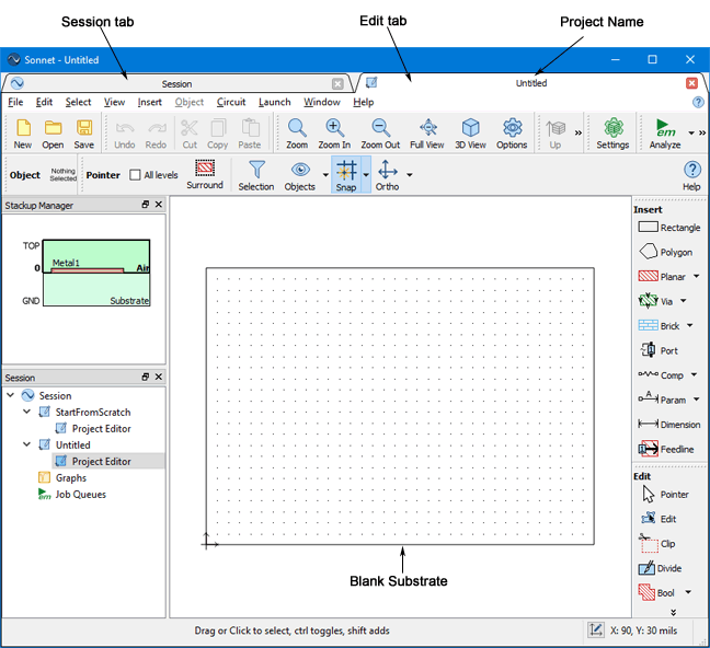
A new Edit tab is opened with a new project displayed. The project editor's interface appears in the Edit tab. The Edit tab is identified with the  icon. The project name is displayed in the tab. Since this is a new geometry which has not yet been named, the tab displays "Untitled." Notice that the Edit tab has been added to the Sonnet session window, which now contains two tabs, the session tab and the edit tab.
- Click on the Edit tab and drag it away from the session window.
The Edit tab appears in a second session window. The original session window now only contains the session tab. While only one session may run at a time, you may open multiple session windows. Each session window may contain one or multiple tabs. Tabs may be pulled away to create another session window and tool bars and panels may be moved within a tab. Any configuration changes are automatically saved when you exit Sonnet.
- In the new window you just created, select Window - Dock tab from the main menu.
The two tabs once again appear in the same session window. For more information on configuring your Sonnet session, please see Reconfiguring Sonnet Windows.
Units
- Click on the Settings button
 in the project editor's Circuit tool bar.
The Circuit Settings dialog box appears on your display. This is a group dialog box with multiple pages which you select by clicking on the entries in the Side bar menu of the dialog box. Most of the setup for your circuit may be performed in this dialog box and the side bar menu may be used as a "checklist" of tasks that need to be done to complete setup.
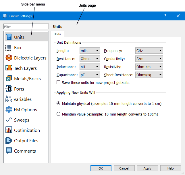
- If it is not already selected, click on Units in the side bar menu to display the Units page.
The Units page sets the measurement units for your circuit. There is no need to specify units when entering values; the units specified here are applied automatically. These are the units we will use for the tutorial so no further action needs to be taken.
Box and Cell Size
The Sonnet EM analysis is performed inside a six-sided metal box as shown below. This box contains any number of dielectric layers which are parallel to the bottom of the box. Metal polygons may be placed on levels between any or all of the dielectric layers, and vias may be used to connect the metal polygons on one level to another.
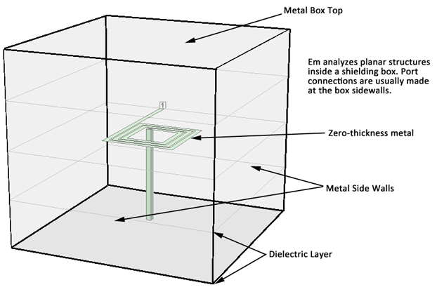
The four sidewalls of the box are lossless metal, which provide several benefits for accurate and efficient high frequency EM analysis:
- The box walls provide a perfect ground reference for the ports. Good ground reference is very important when you need S-parameter data with dynamic ranges that might exceed 50 or 60 dB, and Sonnet’s sidewall ground references make it possible for us to provide S-parameter dynamic range that routinely exceeds 100 dB.
- Because of the underlying EM analysis technique, the box walls and the uniform grid allow us to use fast-Fourier transforms (FFTs) to compute all circuit cross-coupling. FFTs are fast, numerically robust, and map very efficiently to computer processing.
- There are many circuits that are placed inside of housings, and the box walls give us a natural way to consider enclosure effects on circuit behavior.
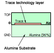
For this tutorial example, a microstrip circuit is modeled in Sonnet by creating two dielectric layers: one which represents your substrate, and one for the air above the substrate. The metal polygons for the microstrip are placed on the metal level between these two dielectric layers. The bottom of the box is used as the ground plane for the microstrip circuit. The top and bottom of the box may have any loss, allowing you to model ground plane loss.
To input a circuit geometry in the project editor, you must set up the box and substrate parameters as well as drawing the circuit. Below is a discussion of some of the factors to consider when setting up the box and cell size.
Specifying the parameters of the enclosing box defines the dimensions of the substrate, since the substrate covers the bottom area of the box. There are three interrelated box size parameters: Cell Size, Box Size, and Number of Cells. Their relationship is as follows:
(Cell Size) X (Num. Cells) = Box Size
Therefore, changing one parameter may automatically cause another parameter to change. Any one of the parameters can be kept constant when changing sizes by locking the value.
The electromagnetic analysis starts by automatically subdividing your circuit into small rectangular subsections. Em uses variable size subsections. Small subsections are used where needed and larger subsections are used where the analysis does not need small subsections.
A “cell” is the basic building block of all subsections, and each subsection is “built” from one or more cells. Thus a subsection may be as small as one cell or may be multiple cells long or wide. Thus the “Dimensions” of a cell determine the minimum subsection size.
The smaller the subsections are made, the more accurate the result is and the longer it takes to get the result. Therefore, there is a trade off between accuracy and processing time to be considered when choosing the cell size. The project editor gives you a measure of control over the subsection size. For a detailed discussion of subsectioning, please see Subsectioning in the Sonnet User’s Guide.
Note that the dimensions of a cell do not need to be a “round” number. For example, if you want to analyze a line that is 9.5 mils wide, you need not set your cell dimension to 0.5 mils. You may want to set it to 4.75 mils (9.5 mils divided by 2) or 3.16667 mils (9.5 mils divided by 3). This will speed up the analysis because fewer subsections will be used. Also, the width of the cell does not need to be the same as the length.
When viewing your substrate, notice that the project editor displays a grid made up of regularly spaced dots. The distance between each grid point is the cell size.
The cell size may be entered directly or you may enter the number of cells. This sets the number of cells per substrate side, thus implicitly specifying the cell size in relationship to the box size. Note that the number of cells must be an integer number.
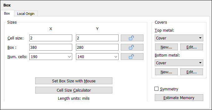
- Click on Box in the side bar menu of the Circuit Settings dialog box.
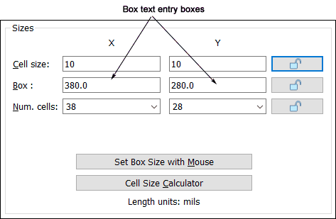
The Box page is displayed. If it is not already selected, click on the Box tab in the Box page. For this circuit, we will set the the box size to 380 mils by 280 mils.
- Enter 380 in the X text entry box in the Box row of the Box page of the Circuit Settings dialog box.
This sets the x dimension of the box, and thereby, the substrate, to 380 mils.
- Enter 280 in the Y text entry box in the Box row of the Box page of the Circuit Settings dialog box.
This sets the Y dimension of the box, and thereby, the substrate, to 280 mils.
Note that when these values are entered, the number of cells value is updated to correspond to the new box size.
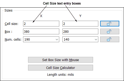
In observing the dimensions of the circuit it can be seen that a common factor of the dimensions, in both the x and y directions, is 2 mils. The feedlines of the filter are 16 mils wide, the resonators are 20 mils wide, and the lengths of the resonators and feedlines are all an even number of mils. In order for all the metalization to fall on the cell grid, a cell size of 2 X 2 mils is used. Off-grid metalization is possible; however, that is addressed elsewhere.
A cell size of 2 mils by 2 mils provides enough accuracy for this circuit while needing the least processing time.
- Enter 2 in the X text entry box in the Cell Size row of the Box page of the Circuit Settings dialog box.
This sets the x dimension of the cell to 2.0 mils.
- Enter 2 in the Y text entry box in the Cell Size row of the Box page of the Circuit Settings dialog box.
This sets the Y dimension of the cell to 2.0 mils. Note that the Num. cells entries are also updated.
Box Cover Metals
Metal in your circuit is modeled using two different classes of metal types: planar and via. Planar metal types are used for metal polygons and box covers (box sides are always modeled using lossless metal). Via metal types are used to model via polygons.
You define what type of metal a box cover or polygon uses by defining metal types in your project, then assigning them to the polygons or a box cover.
There is no limit as to how many different metals are used on any given level or how many metal types you may define for a project. To model loss in your metal, you enter the metal’s loss characteristics when you define the metal type. It is also possible to use a provided library of metal types or define your own metal library to use in multiple projects.
For this tutorial, we use the Gold metal type defined in the Metal library to model the box top cover and box bottom cover (ground plane).
Normally, metal types are defined using the Metals/Bricks page of the Circuit Settings dialog box, but the box page also provides a way to define metal types to assign to your cover metals.
- Click on the New button under Top Metal on the Box page.
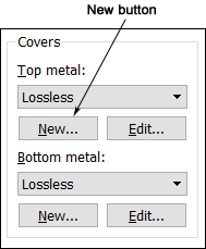
The Metal Editor dialog box appears on your display. This dialog box allows you to define a new metal type.
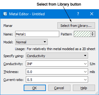
- Click on the Select from Library button in the Metal Editor dialog box.
There are two ways to define your metal type. You may choose a metal model and enter the parameters or you may select a metal definition from a metal library. For this tutorial, we will use a metal type from the library.
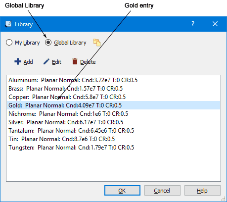
When you click on the Select from Library button, the Library dialog box appears on your display.
- Click on the Gold entry in the list of metals in the Library dialog box.
The Library dialog box is displaying the default Global library delivered with your Sonnet installation. You may also define a local library for your own use or add metal types to to the global library. For more information, please click on the Help button in the Library dialog box.
The Gold Entry is highlighted when you select it. The entry displays the parameters for the metal type.
- Click on the OK button to close the dialog box and apply the metal definition.
The Metal Editor dialog box settings are updated with the parameters defined for Gold in the library.
- Enter "Cover" in the Name text entry box in the Metal Editor dialog box.
This name identifies the metal type in your circuit. There is only one metal type being defined to assign to both the top metal and the bottom metal. Depending on your design, you may wish to assign different metal types to the top and bottom metal.
There is a pattern entry just to the right of the Name entry. A new pattern has been automatically assigned by the software. You may use the up and down arrows to choose another pattern for the metal if you wished to do so. The tutorial uses the default assigned pattern. The metal pattern is used for the metal fill of any polygon in your circuit to which the metal type is defined making it easier to visually identify metal types.
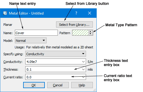
- Enter 0.1 in the Thickness text entry box.
The Normal metal type model, used here, is defined as a zero thickness model. Metal thickness is used only in calculating loss; it does not change the physical thickness of metalization in your circuit.
- Enter "0.0" in the Current Ratio text entry box in the Metal Editor dialog box.
The current ratio is defined as the ratio of the current flowing on the top of the metal to the current flowing on the bottom of the metal at very high frequencies, where the thickness is much greater than a skin depth.
A current ratio of 0 is best for covers since at high frequencies most of the current is on just one side of the metal.
- Click on the OK button in the Metal Editor dialog box to close the dialog box and apply the changes.
The metal type "Cover" is created and applied to the Top Metal. The Box page of the Circuit Settings dialog box is updated to display"Cover" in the Top metal drop list.
- Select "Cover" from the Bottom metal drop list.
The drop list is updated to display "Cover." This applies the "Cover" metal type you just created to the bottom metal of your box. The Box page should appear similar to the picture below.
- Click on the Apply button in the Circuit Settings dialog box.
This saves the changes you just made.
Dielectric Layers
All Sonnet geometry projects are composed of two or more dielectric layers. There is no limit to the number of dielectric layers in a Sonnet geometry project, but each layer must be composed of a single dielectric material. Metal polygons are placed at the interface between any two dielectric layers and are usually modeled as zero-thickness, but can also be modeled using Sonnet’s thick metal model. Vias may also be used to connect metal polygons on one level to metal on another level.
You can use the Stackup Manager or Dielectrics Layers page of the Circuit Setting dialog box, both shown below, to add dielectrics to, or edit the dielectrics in, your circuit. Each time a new dielectric layer is added, a corresponding metal level is also added to the bottom of the new dielectric layer.
This example shows a 3-D drawing of a circuit (with the z-axis exaggerated). Please note that the pictured circuit is not realistic and is used only for purposes of illustrating the box setup.
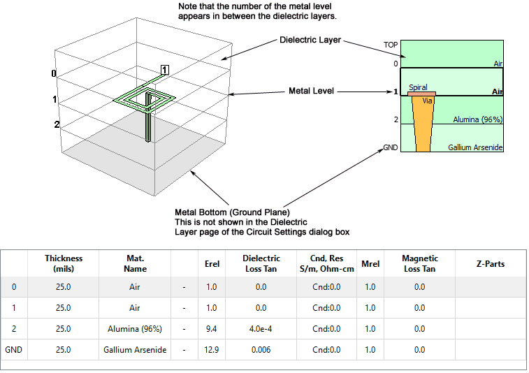
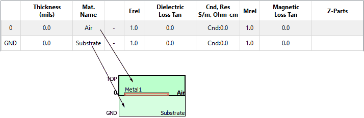
The stackup manager provides a "side" view of your circuit. In our example, the stackup manager displays the two default dielectric layers and default metal technology layer of a new geometry project. The dielectric layers need to be edited.
- Click on "Dielectric Layers' in the side bar menu of the Circuit Settings dialog box.
The Circuit Settings dialog box is updated to display the Dielectric Layers page, which allows specification of the dielectric layers in the box, and provides you with an approximate “side view” of your circuit. You may also see the stackup in the Stackup Manager. The project editor “level” number appears on the left. A “level” is defined as the intersection of any two dielectric layers and is where your circuit metal is placed.
- Click on the Substrate dielectric layer in the Dielectric page of the Circuit Settings dialog box.
This selects the dielectric layer.
- Click on the Edit button
 above the dielectric layer list.
The Dielectric Editor is opened on your display. This dialog box allows you to edit the parameters of the dielectric layer including its thickness.
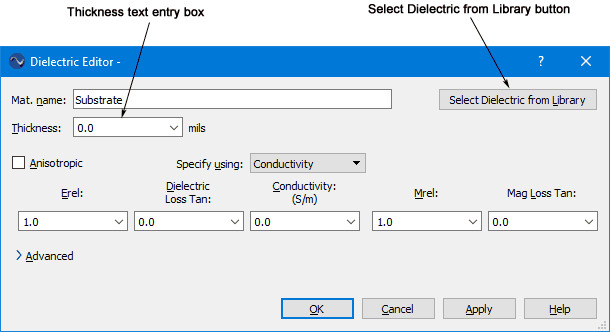
- Click on the Select Dielectric from Library button in the Dielectric Editor dialog box.
The Library dialog box appears on your display. For this dielectric layer, you will chose a dielectric material from the global library provided in your software installation. It is not required to use a dielectric from the library, as it may not contain the material you wish to use. You may edit the dielectric parameters directly to define the material.
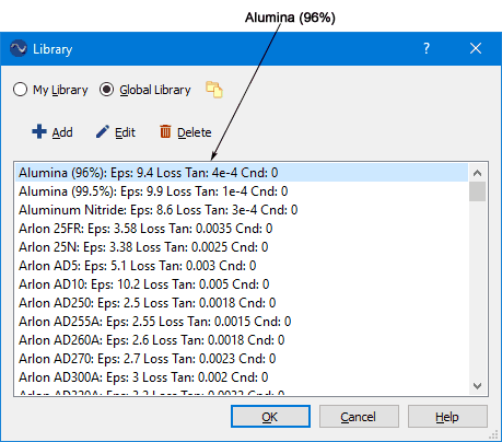
- Click on the Alumina (96%) entry in the Library dialog box to select it.
The entry is highlighted.
- Click on the OK button in the Library dialog box to close the dialog box and apply the changes.
The Dielectric Editor dialog box is updated with the parameters for the alumina.
- Enter "15" in the Thickness text entry box in the Dielectric Editor dialog box.
The substrate is 15 mils thick.
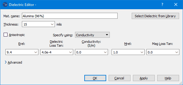
- Click on the OK button in the Dielectric Editor dialog box to close the dialog box and apply the changes.
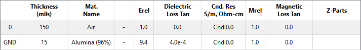
The Dielectric Layers page of the Circuit Settings dialog box is updated with the new parameters for the bottom dielectric layer.
- Click on the Thickness entry in the top dielectric layer in the Dielectrics page.
Selecting the field places it in edit mode. This dielectric layer was defined as Air by default and we want to use a layer of air above the circuit, so there is no need to change any parameters but the thickness, which may be directly edited in the Dielectric Layers page. The air layer needs to be thick enough to move the circuit away from the cover (even if the cover is set to "Free Space."). The topmost dielectric layer should be at least three to five times the substrate thickness.
- Enter "150" in the Thickness entry box in the Dielectric Layers page.
The air layer is set to 150 mils thick. The Dielectric Layers page of the Circuit Settings dialog box is updated and should appear similar to the picture below.
- Click on the Apply button in the Circuit Settings dialog box to save the changes.
This completes the setup of the dielectric layers.
Technology Layers
A Technology Layer allows you to define a group of objects with common properties including the metal level on which they are placed in your Sonnet project. This enables you to more easily control a large group of objects in your circuit and make changes to those objects as efficiently as possible.
Since all the metal polygons in this circuit are the same metal type and all the vias are the same metal type, you will create Technology Layers to manage them. Two different methods of creating a Technology Layer will be demonstrated: using the Circuit Settings dialog box and using the Stackup Manager.
Technology Layers are an optional design element. While a Technology Layer, if created, must be assigned to a level in your project, it is not necessary to have a Technology Layer assigned to every level, or for a project to contain any Technology Layers at all.
- Click on Tech Layers in the side bar menu of the Circuit Settings dialog box.
The appearance of the Circuit Settings dialog box is updated to display the Technology Layers page. The default metal tech layer, Metal1, appears in the list.
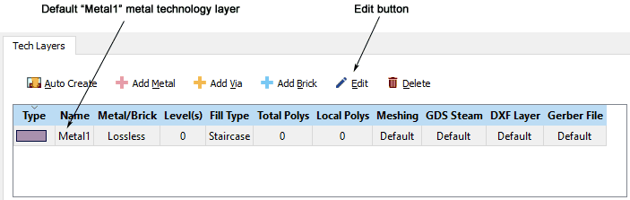
- Click on the Metal1 entry to select it, then click on the Edit button.

The Technology Layer Editor dialog box appears on your display. This dialog box allows you to input or edit the parameters for a technology layer.
- Enter "Trace" in the Name text entry box in the Technology Layer Editor dialog box.
This is the tech layer name that will be displayed in the stackup manager.
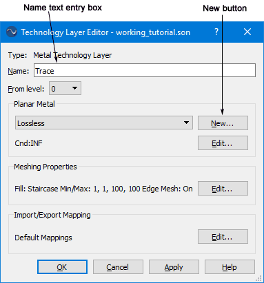
- Click on the New button in the Planar Metal section of the Technology Layer Editor dialog box.
The Metal Editor dialog box appears on your display. You will define a new metal type to be used for the metal technology layer.
- Enter "Gold_Trace" for the Name, "4.09e7" for the Conductivity, "0.1" for the Thickness.
This metal type uses the Normal metal type model which is selected by default.
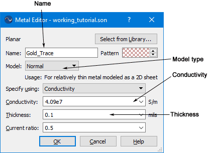
- Click on the OK button in the Metal Editor dialog box to close the dialog box and create the metal type.
The Technology Layer Editor dialog box is updated and now displays "Gold_Trace" as the planar metal type used for this technology layer. No other changes need to be made.
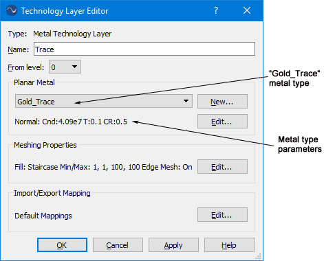
- Click on the OK button in the Technology Layer Editor dialog box to close the dialog box and apply the changes.
The Technology Layers page of the Circuit Settings dialog box is updated and now displays the Trace technology layer.
- Click on the OK button in the Circuit Settings dialog box to close the dialog box and apply the changes.
The project editor window is updated to display the new substrate size and the stackup manager now displays the Trace metal technology layer. The substrate dielectric layer is also updated to display the name Alumina. Note that the stackup manager is not to scale; all dielectric layers are displayed as equal in thickness.
- Right-click on the Alumina dielectric layer in the stackup manager and select "Add Via Tech Layer" from the pop-up menu which appears.
The Technology Layer Editor dialog box appears on your display. Note that this time the Type is a Via Technology Layer. Since you clicked in the lower dielectric, the technology layer defaulted "from" GND "to" metal level 0, which is the correct placement.
- Enter "Via_Gnd" in the Name text entry box in the Technology Layer Editor dialog box.
This is the tech layer name that will be displayed in the stackup manager. As mentioned earlier, the From Level and To Level are already set correctly.
- Click on the New button in the Via Metal section of the Technology Layer Editor dialog box.
The Metal Editor dialog box appears on your display. You will define a new metal type to be used for the via technology layer. This metal type uses the default Volume loss model.
- Enter "Gold_Via" for the Name, "4.09e7" for the Conductivity, "0.1" for the Wall Thickness.
This metal type uses the Wall Thickness for the Volume Properties. This model uses the wall thickness and the shape of each via polygon to determine the cross sectional area for the loss calculations.
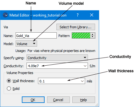
- Click on the OK button to close the dialog box and apply the changes.
The Technology Layer Editor dialog box is updated to show the via metal type you just defined, Gold_Via, as the metal type for the technology layer.
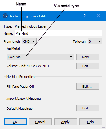
- Click on the OK button in the Technology Layer Editor dialog box to close the dialog box and create the via technology layer.
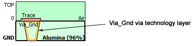
The stackup manager is updated and now shows the Via_Gnd via technology layer. Note that the via technology layer is drawn extending from GND to metal level 0. Please note that it does not make a difference in which direction you define your From level and To Level for a via technology layer. Using 0 as the From Level and GND as the To Level would yield the same result shown here.
This completes setting up your circuit. In the next section, you draw the circuit.
Drawing the Circuit
This section demonstrates how to use the various tools in the project editor to input your circuit. Our metal technology layer is defined as being on level 0. Any metal polygons created on this level are automatically assigned to the metal technology layer Trace.
The bottom dielectric layer is presently selected in the stackup manager. The view of the metal level in the main window is always the metal level below the selected dielectric in the stackup manager, so the present view is of the box bottom (GND).
- Click on the top dielectric layer in the stackup manager to change to the Level 0 view.
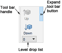
You may also use the Level drop list in the Levels tool bar to change the metal level view. In the default view of the Edit tab, the level drop list may not be visible because the tool bar is truncated due to space restrictions. To access the level drop list, you would click on the >> which displays the whole tool bar. Notice that the present level number is displayed.
Adding a Polygon
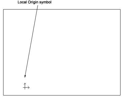
- Click on the Local Origin icon in the status bar of the project editor.

The status bar is located at the bottom of the edit tab. The Local Origin dialog box appears.
- Set the origin to 70,26 by entering "70" in the X entry box and "26" in the Y entry box.
This location is the corner of the first polygon you draw.
- Click on the OK button in the Local Origin dialog box to close the dialog box and apply the changes.
The view of your circuit is updated and the origin symbol is moved to 70,26.
- Click on the Rectangle icon
 in the Insert tool bar.
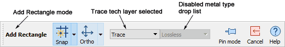
The appearance of your cursor changes to indicate you are in Add Rectangle mode and the Add Rectangle tool bar appears. Because there is already a metal technology layer defined on this level, the tool bar defaults to adding a metal polygon assigned to the Trace technology layer. Since a technology layer is selected, the metal type drop list is disabled.
- Move your cursor over the Local Origin symbol in the circuit view until the symbol is highlighted with a blue circle, then click.
The Local Origin readout in the status bar at the bottom of the Edit tab should read 0,0. This is the first point of your rectangle.
- Type "20,224" on the keyboard, then press the Enter key.
Notice that as you type the value "20,224" the values appear in the X and Y entries on the status bar. Pressing the enter key completed the entry and the first resonator is added to the circuit view. When entering values using your keyboard, you can use the backspace key if you make a mistake.
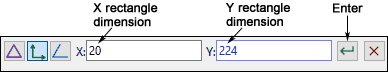
The first resonator is 20 mils by 224 mils. Note the technology layer Trace is now depicted in the stackup manager as a solid color block instead of an outline because the technology layer has a polygon defined.
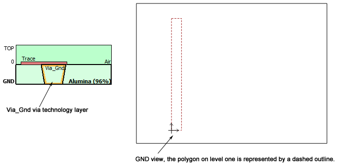
Adding a Via
This circuit connects the resonators to ground. Vias, which are a special kind of subsection which allows current to flow in the z-direction between metal levels, are needed to model the ground connections.
Sonnet vias can be used to connect metal on any level in a circuit to metal on any other level. They are commonly used to model vias to ground, connections to air bridges, and can even be used to approximate wirebonds.
Sonnet vias use a uniform distribution of current along their height and thus are not intended to be used to model electrically long vertical structures. Therefore, the height of the via should be a small fraction of a wavelength.
You are going to create a via near the bottom of the resonator you just drew.
- Click on the via technology layer, Via_Gnd, in the stackup manager.
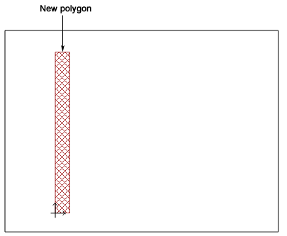
The circuit view changes to the GND level. The resonator you just drew is represented by a dashed outline. Any metal polygons that are on other metal levels in your circuit are shown this way. We selected the via technology layer so that when we add a via polygon, it will default to the technology layer.
- Zoom in on the bottom of the resonator by clicking on your middle mouse button then dragging to enclose the area on which you wish to zoom in.
You could also use the Zoom buttons on the view tool bar. Double-clicking on the middle mouse button returns you to a full view. The circuit view is redrawn to show the zoomed view. It should appear similar to the picture below.
- Select Insert - Via - Circular Via from the main menu of the Edit tab.
The Circle Properties dialog box appears on your display. This dialog box allows you to define the circular via you are adding to your circuit.
- Enter "10" for the diameter.
Click on the field to place it in edit mode, then edit the value and change it to 10. The rest of the default values are appropriate so no further changes need to be made.
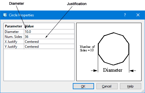
- Click on the OK button to close the dialog box and apply the changes.
When you close the dialog box, an outline of the circular via appears with a blue cross indicating the center of the via. Since both the X Justify and Y Justify were set to "Centered" the middle of the via is placed where you click your mouse.
- Move your cursor until the readout in the status bar is 10,10, then click your mouse.
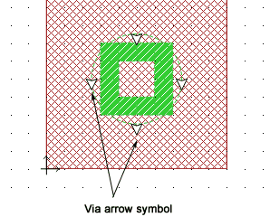
These values are relative to the local origin, which is at the corner of our resonator. This places the via in the resonator. The via is added to your view. Notice that there is a outline representing the via you just specified but the metal fill, showing the actual metal analyzed by em, is a thick green rectangle. By default, Sonnet uses a Ring meshing fill for new via polygons, which places via subsections along the entire perimeter of the via polygon with a hollow center. This perimeter is always one cell wide. Other types of meshing fill may be assigned once the via polygon is added to your circuit. The default Ring meshing fill is used in this example.

- Go up one level to view metal level 0.
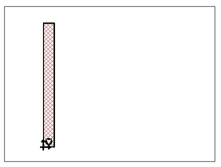
You may do this by clicking on the top dielectric layer in the stackup manager or by clicking on the Up button in the Level tool bar or using the up arrow key. The circuit view is updated. This view shows the top of the via. This via was automatically assigned to the via technology layer, Via_Gnd, so that the via extends from the GND level upward to level 0. Note that the via arrows on the GND level are pointing upward, but the via arrows on level 0 are pointing downward.
- Click on the Full View button
 in the View tool bar.
The full circuit view is displayed. As mentioned earlier, you could also double-click the middle mouse button to return to the full view.
Next, you will copy and move the existing resonator and via to create the rest of the filter.
- Click and drag your mouse to select the resonator and via.
The resonator and via are highlighted.
- Select Object - Move from the project editor main menu.
The Move dialog box appears on your display.
- Select the Make a Copy checkbox.
This will make a copy, then move the copy the specified distance from the present location.
- Enter "50" in the X delta text entry box and "0" in the Y delta text entry box.
The copy will be moved 50 mils in the X-direction. We do not want to move the copy in the Y direction, so that value is set to zero.
- Click on the Apply button to copy the resonator and move it 50 mils.
A second resonator and via pair is added to your circuit view. The new resonator is still selected. Clicking on the Apply button left the Move dialog box open so that we can continue to copy the resonators.
- Enter "60" in the X delta text entry box and click on the Apply button.
A third resonator is created 60 mils away from the second resonator.
- Enter "60" in the X delta text entry box and click on the Apply button.
A fourth resonator is created 60 mils away from the third resonator.
- Enter "50" in the X delta text entry box and click on OK.
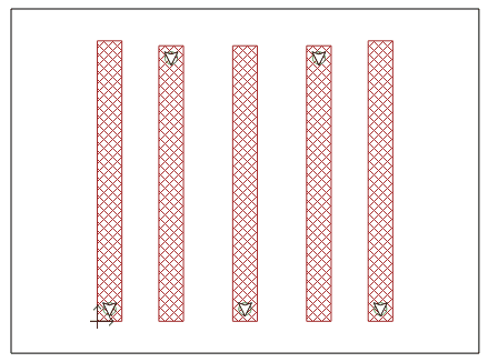
A fifth resonator is created 50-mils away from fourth resonator. Since this is the last resonator we wish to add, we click on the OK button to also close the dialog box in addition to creating the fifth resonator. Your circuit should appear similar to the picture below.
Next, the height of the first and last resonator needs to be increased by 4 mils (2 cells).
- Zoom in on the top of the first resonator by clicking the Zoom button
 on the tool bar, then select an area around the top of the resonator.
You should in enough to be able to see the dots indicating the grid.
- Click on the resonator to select it.
Edit handles and points in the form of a square and circles appear when the resonator is selected. These controls allow you to quickly and intuitively change your polygons.
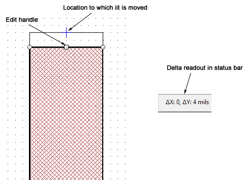
- Click on the Edit handle (the square in the middle of the top edge) and drag it upward for two cells (two tics on the grid).
When you are dragging the Edit handle, a delta readout appears in the status bar, as shown below. This allows you to ensure you are moving the handle by 4 mils.
- In a similar manner extend the height of the last resonator.
Next, we will move the vias on the second and fourth resonators.
- Go to full view and click on the via on the second resonator to select it.
The via is highlighted with a black circle.
- Hold down the Shift key and click on the via on the fourth resonator to select.
Holding down the shift key selects this via without de-selecting the first via. Both vias are now highlighted.
- Type "@0,204" on the keyboard, then press the Enter key.
Both vias are moved 204 mils in the Y direction and are now close to the top of the resonators. Using the @ symbol indicates a relative move command. As before, the entry appears in the status bar. Relative move keyboard commands can be used for many editing actions including moving polygons, moving points, adding polygons and adding rectangles. See Keyboard Entry of Points and Polygons for more information.
The circuit should now appear as shown below.
Next, you need to add tap-lines to each end of the filter. You will create the tap-line by creating a rectangle polygon, then a taper polygon and combining the two polygons.
- Click on the Local Origin icon in the status bar of the project editor.
The status bar appears at the bottom of the edit tab. The Local Origin dialog box appears.
- Set the origin to 0,66 by entering "0" in the X entry box and "66" in the Y entry box.
This location is the corner of the first tap-line you draw.
- Click on the OK button to close the dialog box and apply the changes.
- Click on the Rectangle icon in the Insert tool bar.
The appearance of your cursor changes to indicate you are in Add Rectangle mode and the Add Rectangle tool bar appears. Because there is already a metal technology layer defined on this level, the tool bar defaults to adding a metal polygon assigned to the Trace technology layer. Since a technology layer is selected, the metal type drop list is disabled.
- Move your cursor over the Local Origin symbol in the circuit view until the symbol is highlighted with a blue circle, then click.
The Local Origin readout in the status bar at the bottom of the Edit tab should read 0,0. This is the first point of your rectangle.
- Type "62,16" on the keyboard, then press the Enter key.
The values appear in the X and Y entries on the status bar. You could have defined the polygon by clicking on and directly editing these entries. Pressing the enter key completed the entry and the left tap-line rectangular polygon. The polygon is 62 mils by 16 mils.
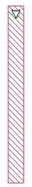
- Zoom in on the gap between the left tap-line polygon and first resonator.
The magnification should be sufficient to show the cell grid.
- Click on the Insert Polygon icon
 in the Insert tool bar.
The Add Polygon tool bar appears. Similar to the rectangle, this polygon defaults to the Trace metal technology layer.
- Click on the bottom right hand corner of the tap-line rectangle you just drew.
This is the first point of the polygon.
- Click on the resonator edge up three cells from your starting point.
If you make a mistake and click on the wrong point, you may press the delete key to remove the last point added, then continue inputting the polygon.
- Click on the resonator edge up two cells from the previous point.
- Click on the upper left hand corner of the tap-line rectangle.
- Click again on the starting point to complete the polygon.
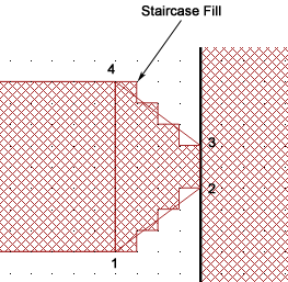
You may also double-click your mouse after the fourth vertex to complete the polygon. The taper is drawn in your circuit view. When a polygon is complete, a fill pattern which defines the actual metalization analyzed by em appears on your display. In the picture above, notice the staircase approximation for the taper edge. Em does not analyze the taper as you entered it; the staircase approximation is analyzed instead.
- Select the tap-line rectangle and the taper polygon.
To do so, click on the rectangle polygon to select it, then hold down the shift key and click on the taper polygon.
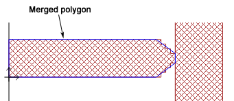
- Select Edit - Boolean Operations - Union from the project editor main menu.
The two polygons are combined into one polygon. Note that combining the polygons is not necessary, but a single polygon is easier to work with in the next step.
- Go to a full view and click on the taper polygon to select it.
To create the right hand tap-line, you will copy and flip the left hand one you just created.
- Select Object - Flip from the project editor main menu.
The Flip dialog box appears on your display.
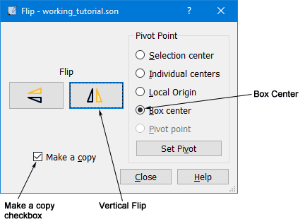
- Click on the "Make a copy" checkbox.
When the flip is performed, the original polygon remains the same. A copy is created and flipped.
- Click on the Box center radio button for the pivot point.
Performing the flip using the box center as the pivot point will position the copy on the other box wall.
- Click on the Vertical Flip button
 in the Flip dialog box.
A flipped copy of the tapered polygon is created, correctly positioned between the fifth resonator and the right box wall.
- Drag the local origin symbol to the bottom left hand corner of the substrate.
It is possible to change the location of the local origin by dragging it to a new position. The bottom left hand corner of the substrate is 0,0.
Metal Types
The project editor allows you to define any number of metal types to be used in your circuit. A planar metal type specifies the metalization loss used by em. Both the DC resistivity and the skin effect surface impedance are accurately modeled in em. For a detailed discussion of metal types and loss, see Metalization and Dielectric Layer Loss in the Sonnet User’s Guide.
After a polygon is drawn in your circuit, you can change the planar metal type. You can do this by creating another Technology Layer that uses another metal type or by making the polygon independent or local. In our example, all the polygons are included in the Trace technology layer which uses the Gold_trace metal type. An example is given below of changing the polygon to independent and the planar metal type of one polygon to “Lossless” metal. This change is done here for the purpose of demonstration; the metal type of the polygon will be changed back before analyzing.
- Click on any resonator of the filter to select it.
The polygon is highlighted to indicate selection.
- Select Object - Metal Properties from the main menu of the project editor.
The Planar Polygon Properties dialog box appears on your display as shown below.
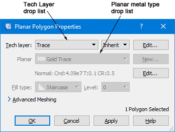
- Select <None> from the Tech Layers drop list.
This removes the selected polygon from the Technology Layer and makes it independent. The controls in the dialog box are enabled.
- Click on the Planar drop list and select “Lossless” from the list. Click on the OK button to apply the change and close the dialog box.
The fill pattern changes for the selected polygon as shown below.
The metal for this polygon now has the loss associated with the default lossless planar metal. The project editor allows you to define any number of metal types for use in your circuit.
- Double-click on the lossless resonator.
The Planar Polygon Properties dialog box appears on your display. Double-clicking on objects in your circuit opens up the appropriate properties dialog box.
- Select "Trace" from the Tech layer drop list and click on OK to close the dialog box and apply the changes.
This assigns the polygon to the Trace metal technology layer again. The metal fill pattern is updated to indicate that the polygon is using the Gold_trace planar metal type.
Metal Fill
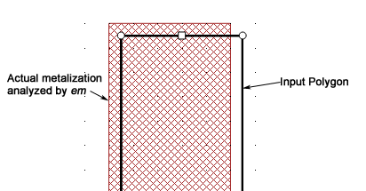
Metal polygons are represented with an outline and a cell fill pattern. The outline represents exactly what you entered or imported. The cell fill represents the actual metalization analyzed by em. Therefore, the actual metalization analyzed by em may differ from that input by you.You turn the cell fill on and off using the control-M key. This next section demonstrates what happens when your circuit falls "off" the grid.
- Click on the Settings icon in the tool bar.
The Circuit Setting dialog box appears on your display.
- Click on Box in the side bar menu, and if it is not already selected, click on the Box tab in the Box page.
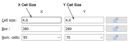
- Enter "4" in the X Cell Size and "4" in the Y Cell Size.
This will increase the cell size from 2 by 2 mils to 4 by 4 mils.
- Click on the OK button in the Circuit Settings dialog box to close the dialog box and apply the changes.
The circuit is redrawn using the new cell size. If you zoom in on the top of the first resonator, you will notice that the metal polygon is no longer “on” grid. In this case, since the dimensions you entered for your resonator no longer fit exactly on the grid as they did with the smaller cell size, there is now a slight difference between the input polygon (black highlight) and the actual metalization (cross hatched area) analyzed by em. For more information on choosing a cell size, see Tips for Selecting a Good Cell Size in the Sonnet User's Guide.
- In the same manner, change the cell size back to 2 by 2 mils and then go to the full view.
The circuit is updated and once again falls on the grid so that the metal fill matches the input polygons.
Adding Ports
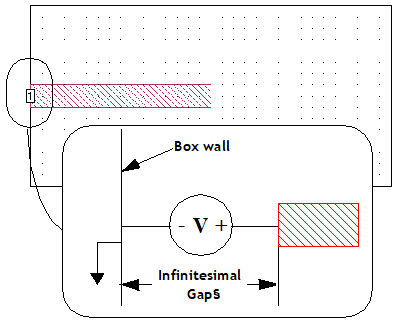
Circuits in Sonnet are modeled as being enclosed in a six-sided metal box which is treated as ground unless special port numbering is used.. Any metal polygon touching the box is shorted to the box unless the polygon has a port attached to it. A standard box wall port is a grounded port, with one terminal attached to a polygon edge coincident with a box wall and the second terminal attached to ground. The port, therefore, breaks the connection between the polygon and the wall and is inserted in an “infinitesimal” gap between the polygon and the wall. The signal (plus) terminal of the port goes to the polygon, while the ground (negative) terminal of the port is attached to the box wall (ground). The model for a box wall port is pictured below.
- Holding down the shift key, click on the Port icon
 in the Insert tool bar.
Holding down the shift key, leaves you in Add Port mode until you explicitly exit the mode. This allows you to insert multiple ports without having to click on the tool bar each time.
- Click on the left end of the left tap-line at the box wall.
A box wall port is added to your circuit. The port type is automatically determined based on placement. Their are different symbols for different port types, see Insert - Port for more information.
- Click on the right end of the right tap-line at the box wall.
Another box wall port is added to your circuit. Notice that the ports are automatically numbered in the order in which they are created.
This completes the input of your circuit. Next, we will set up the analysis.
Analysis Setup
- Click on the Settings icon in the tool bar.
The Circuit Setting dialog box appears on your display.
- Click on Sweeps in the side bar menu of the Circuit Settings dialog box.
The Circuit Settings dialog box is updated to display the Sweeps page. The default ABS sweep is already displayed in Sweep Set 1. An ABS sweep uses the Adaptive Band Synthesis (ABS) technique to perform a fine resolution analysis of a specified frequency band by analyzing at a small number of discrete frequencies then determining a rational polynomial fit to the S-parameter data to synthesize the rest of the response data. For a detailed discussion of Adaptive Band Synthesis, see the Adaptive Band Synthesis (ABS) chapter in the Sonnet User's Guide.
- Double-click on the ABS entry to set up the sweep.
The display is updated with entry boxes for the ABS band.
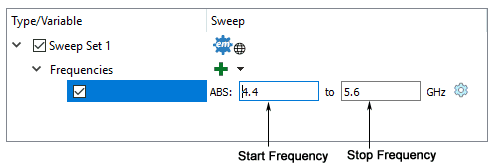
- Enter "4.4" as the Start frequency and "5.6" for the Stop Frequency.
The analysis band is from 4.4 GHz to 5.6 GHz.
- Click on the Apply button in the Circuit Settings dialog box to save the sweep.
This is not necessary as the sweep changes would be applied when you click on the OK button later to close the dialog box, but is done as a precaution.
- Click on the EM Options in the side bar menu of the Circuit Settings dialog box.
The dialog box is updated to display the EM Options page of the Circuit Settings dialog box
- Select the Compute Currents checkbox in the EM Options page.
This option outputs current density information for the entire circuit which can be viewed using the current density viewer, which we do later in this tutorial. For an ABS sweep, current density data is only computed at the discrete data points where a full analysis is performed. If you need current density at all frequency points, you should use a linear sweep.
You should be aware that calculating current density data can increase the time needed for your analysis.
- Click on the OK button in the Circuit Settings dialog box to close the dialog box and apply the changes.
The circuit setup is complete but the project needs to be saved before performing an analysis.
- Click on the Save icon
 in the File tool bar in the Edit tab.
Since this is the first time you have saved the project, a browse window appears to allow you to enter a name for the project. Save the project in your working directory using the name "my_tutorial.son."
Em, the Analysis Engine
In the next section of the tutorial, the circuit you entered is analyzed using the electromagnetic simulator engine, em. The following discussion provides background on em and explains the theory behind the analysis engine.
The analysis engine, em, performs electromagnetic analyses for arbitrary 3-D planar geometries, maintaining full accuracy at all frequencies. Em is a “full-wave” analysis engine which takes into account all possible coupling mechanisms.
Em performs an electromagnetic analysis of a microstrip, stripline, coplanar waveguide, or any other 3-D planar circuit, by solving for the current distribution on the circuit metalization using the Method of Moments.
Subsectioning the Circuit
The analysis starts by subdividing the circuit metalization into small rectangular subsections. In an actual subsectioning, shown below, small subsections are used only where needed. Otherwise, larger subsections are used since the analysis time is directly related to the number of subsections. These subsections are based on the cells specified in the geometry file.
Em effectively calculates the “coupling” between each possible pair of subsections in the circuit.
- Select Circuit - Estimate Memory from the project editor main menu.
The Estimate Memory window appears on your display. The command subsections your circuit and displays a memory estimate for your analysis. This command can help you determine if you have the computer resources available to run your analysis.
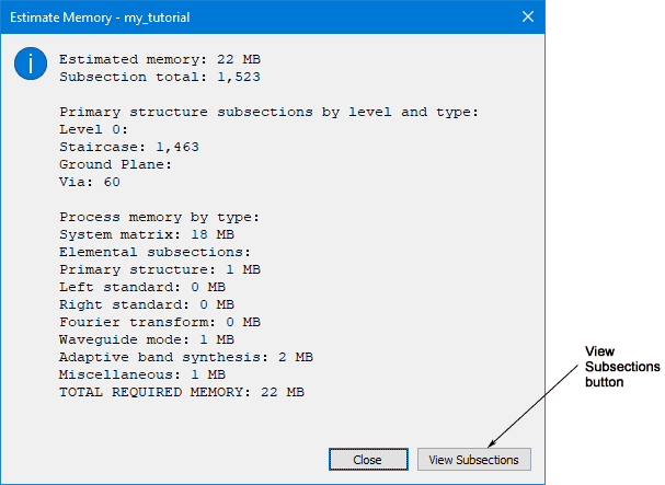
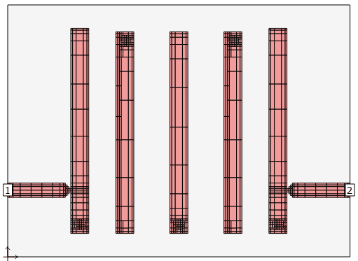
- Click on the View Subsections button in the Estimate Memory window.
A Subsection viewer tab is opened in your session window, displaying the subsectioning for your circuit. Note that the via subsections are not visible on Level 0 but if you view the GND level you can see them.
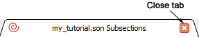
- Close the Subsection viewer tab by clicking on the red x in the corner of the tab.
The tab is closed.
Analyses are set up in the job queue tab. The job queue tab provides an interface that allows you to monitor analyses and manage queues for running analyses. Your analysis control settings are saved as part of your project file.
- In the Edit tab, click on the Analyze button in the Launch tool bar.

A job queue tab appears in your session window. If you have multiple analysis servers defined, you will be prompted as to which server you wish to assign to this queue.
Analyses are set up in the job queue tab. The job queue tab provides an interface that allows you to monitor analyses and manage queues for running analyses. Your analysis control settings are saved as part of your project file.
This project, my_tutorial.son, appears in the queue list with a  icon showing that the analysis has not yet run. Because this job queue tab is set to Manual by default, the analysis does not start running until you click on the Run button.
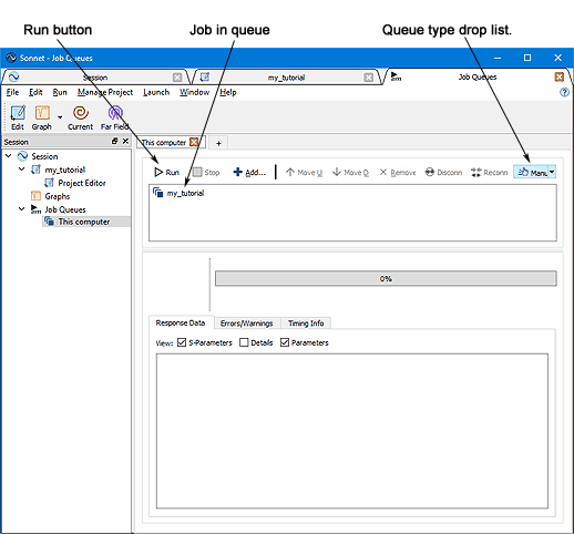
- Select "Auto Start" from the Queue type drop list.
An automatic queue starts running the analysis as soon as a job is loaded in the queue. All job queues open subsequently will be set to automatic until you choose Manual Start from the Queue type drop list. Note that the change to Auto Start does not affect the present queue. You still have to start the analysis job.
- Click on the Run button above the job queue to start your analysis job.
The analysis starts running indicated by the  icon in front of your job. The progress bar appears in the job queue tab to allow you to keep track of the analysis. Status data is output in the window below. When the the job is complete, the message "Em simulation completed" appears below the progress bar. The icon in front of your job is changed to
  to indicate the analysis is complete.
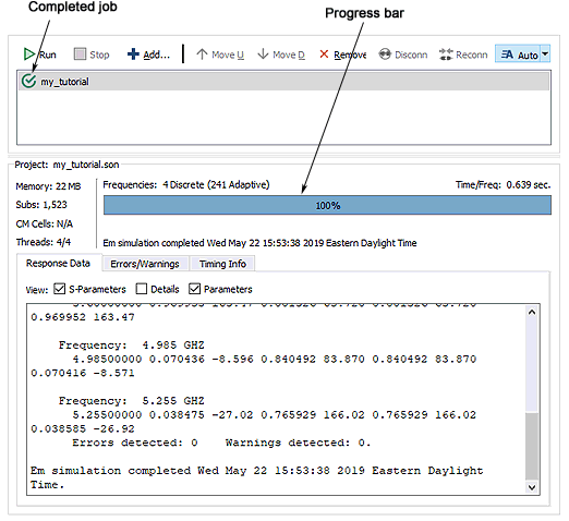
Note that four discrete data points were analyzed to produce 241 adaptive points.
Response Viewer - Plotting Your Data
The response viewer is used to display the results from an em analysis as either a Cartesian graph or Smith chart. S-, Y- and Z-parameters can be displayed alone or simultaneously as well as many other types o measurements. You can also display multiple curves from multiple projects on a single plot or choose to open multiple plots at the same time. It is also possible to display parameter sweeps and optimization results in a number of advanced ways. This tutorial covers only the most basic of the response viewer’s functions.
- Select Launch - Graph Response - New Graph from the main menu in the job queue.
A graph tab with the default measurement of S11 displayed appears in your session window. You can also click on the Graph button  in the Launch tool bar to open a Graph tab.
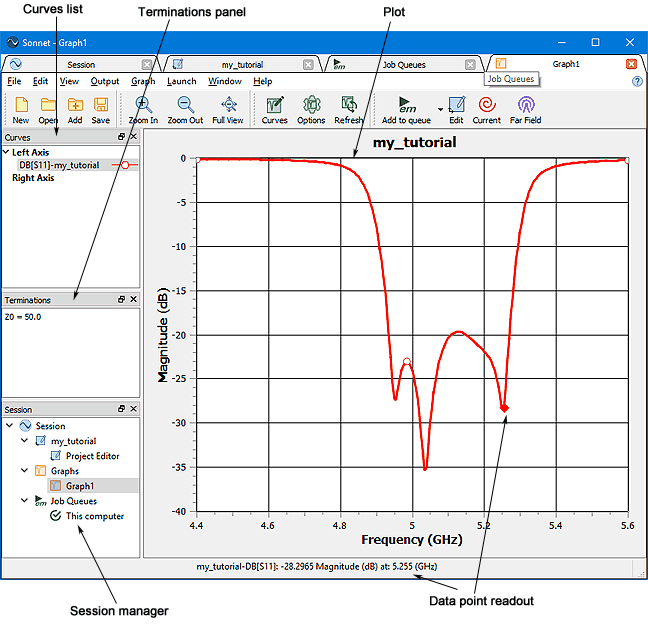
The DB[S11] curve appears in the curve list and identifies the data in the plot. Note that the project name is also used to identify the curve. This is helpful if you are plotting data from more than one project. A selected point in the plot is highlighted using a red square; the data for that point is displayed in the status bar at the bottom of the tab. Points in the plot with a circle symbol represent the discrete data point; a symbol is not used for adaptive data points.
Notice that the session manager is also updated and all of your open tabs are listed in the session manager tree. Since the graph tab is presently the displayed tab in the session window, its entry is highlighted in the session manager. Clicking on another entry displays that tab in the session window.
For more details about the Graph tab, select Help - Help on this tab from the main menu.
- Click on the Curves icon
 in the tool bar.
The Manage Curves dialog box appears on your display. This dialog box allows you to add and edit curves and manage curve groups. Next, we add a DB[S21] curve to the plot.
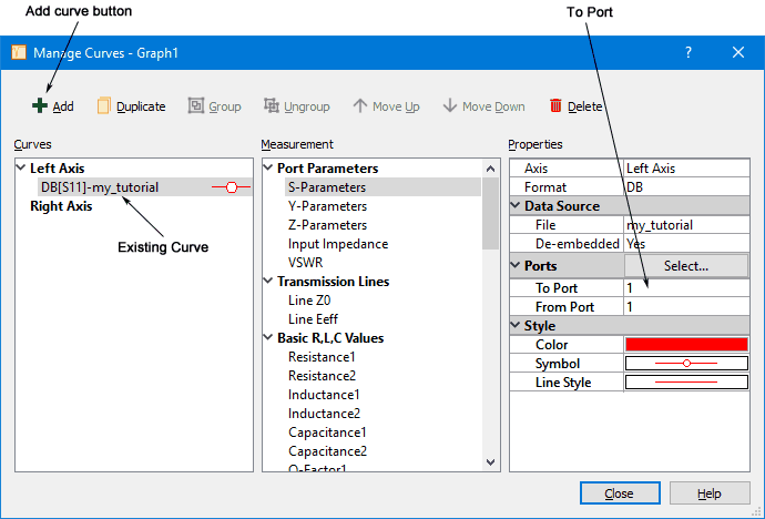
- Click on the Add button in the Manage Curves dialog box.
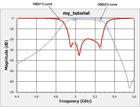
Another DB[S11] curve is added to the list. The new curve is selected in the list (highlighted in gray), so any changes made in the Measurements or Properties sections apply to this curve. Since we want to add another S-parameter, no changes need to be made in the Measurements. Note that a new color was automatically assigned to this curve, but may be changed in the Properties section.
- In the Properties section, click on the To Port field to enable editing.
The entry is highlighted and a small down arrow appears on the left side.
- Click on the down arrow and select "2" from the drop list.
The Properties now define the DB[S21] curve which has also been added to the plot.
- In the Manage Curves dialog box, click on the Delete button.
This deletes the DB[S21] curve you just added since it was still the selected curve. The plot is updated to display only the DB[S11] curve. The DB[S11] curve is now selected in the Curves section.
- Click on the Line Z0 measurement in the Transmission Lines section of the Measurements list.
The Curve entry is updated to MAG[PZ1]. The default settings in Properties are all correct so no further changes need to be made. The plot is also updated.
 In Windows and Linux, hovering over a measurement in the Manage Curves dialog box displays a short description of the measurement. In Windows, you may click on the ? in the title bar of the dialog box, then click on a Measurement entry to get a more detailed description.
- Click on the Close button in the Manage Curves dialog box to close it.
- Select View - Smith Chart from the response viewer main menu.
A new tab appears in your session window displaying a Smith chart of S11.
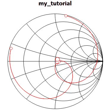
- Click on the Red X and close the Smith chart tab.
Current Density Viewer
The current density viewer is a visualization tool used to view the results of circuits previously analyzed with em. Em saves the resulting current density information in the project file ready for input to the current density viewer.
To produce the current density data, you must select the Compute Current Density option in the EM Options page of the Circuit Settings dialog box which was done earlier in the tutorial.
- Click on the Current button
 in the Launch tool bar.
A current density tab is opened with a plot of the current density data for your project with the first frequency of 4.4 GHz displayed. You are viewing the magnitude of the current density with a 1 Volt, 50 ohm source on Port 1 and a 50 ohm load on Port 2. This is the default setting, but may be changed to any combination of voltages and loads. Red areas represent high current density, and blue areas represent low current density. A scale is shown in the Scale panel which defines the values of each color.
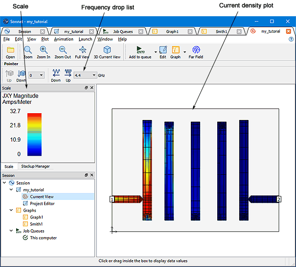
- Click on any point on your circuit to see a current density value.
The current density value (in amps/meter) at the point that you clicked is shown in the status bar at the bottom of your window along with the coordinates of the location.

- Click on the Next Frequency button
 on the tool bar.
When you opened the plot, the lowest frequency appeared on your display as the default, which in this case is at 4.4 GHz. When you click on the Next Frequency button, the display is updated with the current density at 4.985 GHz.
- Click on the Frequency Drop list, and select 5.6.
The drop list allows you to go directly to any of the analysis frequencies. As mentioned earlier in the tutorial, the discrete data points in an ABS analysis for which the current density data is calculated, are determined by the ABS algorithm and are usually non-uniform.
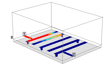
- Click on the 3D Current View button
 in the tool bar of the current density viewer.
A new tab is opened displaying a 3D view of your current density plot. By default, the 3D view is opened in Rotate mode. You can click and drag your mouse to rotate the view in three dimensions.
- Select File - Exit Sonnet from the main menu of any tab.
The software is closed. The next time you open the software, the tabs that were open when you selected the exit command will appear. This concludes the Sonnet tutorial.