Tutorial: Circuit Settings
This part of the tutorial teaches how to start with a blank project and enter your circuit settings. Circuit settings include your measurement units, Analysis Box settings, the cell size, materials, dielectric layer stackup, Tech Layers, frequency sweep values, and the EM options.
Create New Project
For this tutorial, you will start with a new blank project.
Select File > New Geometry from main Sonnet menu.
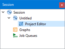
A new Project Editor tab is opened with a new blank Geometry project displayed. The project name is displayed in the tab. Since this is a new Geometry project which has not yet been named, the tab displays "Untitled." Notice that the Project Editor tab has been added to the Session panel.
Select File > Save As.
A browse window appears.
Navigate to a location on your computer where you wish to save your project.
Enter a name for your project and click the Save button.
You may choose any name, but for the purposes of this tutorial, we recommend using the name "part1_settings.sonx" to indicate the stage of the tutorial in which it was created.
Circuit Settings
You will now enter the circuit settings using the Circuit Settings dialog box which is accessed by selecting Circuit > Settings in the Project Editor. The left pane of this dialog box contains buttons which change the contents of the right pane.
Units
The same project units are used throughout your project. For example, if your project's length units are set to microns, all length measurements will be in microns, including polygon dimensions, dielectric layer thicknesses, metal thicknesses, etc. For this tutorial, you will use all of the default units except for the length units. We will be using length units of millimeters.
Select Circuit > Settings > [Units].
The Units pane is opened.
Click the Length drop-down list and select "mm".
All other values may be left at their default values.
You can change your default units by selecting Edit > Preferences > [New Project]. See New Project for details.
Applying New Units
The Applying New Units Will section contains two options. Since this is a newly created project, it does not matter which one you choose. However, if you had already entered values which used any units that you changed here, the radio buttons in the Applying New Units Will section would determine how your changes to the units would affect previously entered values.
- Maintain Physical: If you choose to keep it the same physical size, all distances are converted to the new unit. For instance, if a square is 10 mm on a side and you change the unit to centimeters, it now measures 1 cm by 1 cm.
- Maintain Value: If you choose to allow the circuit to change size, distances retain the same numerical value, but the unit changes. For example, if a distance is 10 mm and you change the unit to meters, the distance is now 10 meters. This option is particularly useful if you have already entered a significant portion of your circuit with the wrong length unit selected.
Your units are now set up.
Box Settings and Cell Size
The size of the Analysis Box is related to the cell size, so we will change them at the same time.
Click the [Box] button in the left pane of the Circuit Settings dialog box.
The Box pane is displayed.
If the Box tab is not selected, click the Box tab.
The Box tab allows you to specify the cell size and box dimensions. The box must always be an integer number of cells in both x and y directions.
Enter 0.1 and 0.1 for the X and Y Cell sizes.
Our spiral inductor will have lines that are 0.6 mm wide and are separated by 0.6 mm. Therefore, an optimal cell size would be one that is a factor of 0.6 mm (0.6 mm, 0.3 mm, 0.2 mm, 0.1 mm, etc.). We will use 0.1 mm by 0.1 mm. See Tips for Determining a Good Cell Size for a more thorough discussion of determining a good cell size.
Enter 20 and 20 for the X and Y Box size.
Since the box sidewalls are perfect electric conductors, they should be kept far away from the spiral inductor metal. The spiral inductor will be about 6 mm by 6 mm, so a 20 mm by 20 mm box leaves about 7 mm between the spiral inductor metal and the box walls.
Click the Covers tab.
The top and bottom covers of the Analysis Box may be set to any impedance. In our case, the spiral inductor will be modeled in an unshielded environment, so the top cover impedance should be set to the impedance of free space. In addition, the bottom cover of the box will act as a copper ground plane for the spiral inductor.
In the Top section, select Free Space from the Conductor drop-down list.
When set to Free Space, the top cover is set to the impedance of free space (approximately 377 ohms per square). This approximates an unshielded environment, provided the Analysis Box sidewalls are far away from the spiral inductor.
In the Bottom section, click New.
The Conductor Properties dialog box appears, allowing you to create a new material to be used for the bottom cover. In our case, the bottom cover will be a copper ground plane. We will use a predefined material that is included in the Installed Library.
Click the Select conductor from Library button.
The Conductor Library dialog box appears. Your Sonnet installation includes an "Installed Library", and also provides the capability to create your own "User Library". See Material Libraries for more details.
If it is not already selected, click the Installed Library radio button.
The Installed Library contains a list of commonly used conductor materials.
You may hover your cursor over each material to see a tooltip that explains the details of the conductor, including the source from which the values were taken.
Select the Copper (annealed) conductor material.
Click OK.
The conductor properties are automatically entered into the Conductor Properties dialog box. In addition, annealed copper is added to your list of available materials. So, you may now use annealed copper for other purposes such as metal traces.
If your particular conductor material is not included in the library, you may enter the properties manually.
Click OK.
The Bottom cover is set to annealed copper.
Enter 0.042 in the Thickness text entry box.
The ground plane thickness is set to 0.042 mm, which represents the combination of ½ oz. copper (0.017 mm) and additional metal plating (0.025 mm). We will assume the copper is perfectly smooth, so you should leave the Roughness value at 0.0 microns.
Your Analysis Box and Cell Size are now set up. At this point, you may wish to save your project. If you wish to do so, click OK, save your project, then select Edit > Circuit Settings to return to the Circuit Settings dialog box.
Materials
You will now define the conductor and dielectric materials used in your project.
Click the [Materials] button in the left pane of the Circuit Settings dialog box.
The Materials pane is displayed. Materials are classified as either conductors or dielectrics.
If it is not already selected, click the Conductors tab.
You should see two conductor entries: The "Perfect Conductor" material is a perfect electric conductor (lossless) and is always in the list. You created the "Copper (annealed)" material when you set up the bottom box cover.
We will be using the annealed copper material for all of our traces, so we do not need to enter any more conductors. However, if you needed to add a new conductor, you could do so by clicking the  Add button.
Click the Dielectrics tab.
The Dielectrics tab contains a list of dielectrics available to your project. By default, two dielectrics, "Air" and "Substrate" are provided. The Air dielectric is always in the list and may not be modified. The Substrate dielectric has the properties of air, but may be modified by you. You may also add new dielectric materials. Our spiral inductor requires Air and FR-4.
Click the Add button to add a new dielectric material.
This opens the properties for the new dielectric material. You could enter the properties directly here, or you could select a dielectric from the dielectric library. We will use the dielectric library.
Click the Select Dielectric from Library button.
This opens the Dielectric Library dialog box. Your Sonnet installation includes an "Installed Library", and also provides the capability to create your own "User Library". See Material Libraries for more details.
If it is not already selected, click the Installed Library radio button.
The Installed Library contains a tree view of commonly used dielectric materials. Clicking the ">" expands a branch of the tree.
The Installed Library contains a large number of materials. It is grouped by vendor, with non-vendor materials grouped under the "Generic" category. To help you navigate the list, you may wish to click the Expand All and/or the Collapse All buttons.
In the Generic category, hover your cursor over the FR-4 entry.
A tooltip appears, explaining that the properties of FR-4 vary depending on the manufacturer. For best results when using dielectrics in the Generic category, you should obtain the dielectric properties from the manufacturer for your particular dielectric(s).
Select FR-4 from the list and click OK.
The dielectric properties are automatically entered into the Dielectric Material Properties dialog box.
Click OK.
FR-4 is added to your list of dielectric materials.
You could have used the Add From Library button instead of the Add button followed by the Select Dielectric from Library button to save an extra step.
Select the Substrate dielectric and click the Delete button.
A message appears, warning you that the Substrate material is being used and Air will be used instead. You will be replacing Air with FR-4 in a future step, so you can ignore this message.
Click the Delete button to delete the Substrate material.
The spiral inductor circuit will not use the material called "Substrate". It is not necessary to delete it, but we are deleting it to keep things clean.
You should now have two dielectric materials defined: Air, and FR-4.
Your conductor and dielectric materials are now complete.
Dielectric Layers
All Sonnet geometry projects are composed of two or more dielectric layers. There is no limit to the number of dielectric layers in a Sonnet geometry project, but each layer must be composed of a single dielectric material. Polygons are placed at the interface between any two dielectric layers. These polygons may represent planar metal, Dielectric Bricks, or vias.
The interface between two dielectric layers is called a "level". Levels are numbered, starting at 0 as shown in the example below.
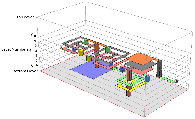
An LTCC circuit containing 8 dielectric layers (including air on top). Polygons are placed on levels 0-6.
The spiral inductor example requires three dielectric layers: two FR-4 layers and a top layer of air. A new project contains only two dielectric layers. You will modify the two existing dielectric layers and add a third in the following steps.You can use the Stackup Manager or Dielectrics Layers pane of the Circuit Settings dialog box to add dielectrics. You will use the latter method in this tutorial.
Click the [Dielectric Layers] button in the left pane of the Circuit Settings dialog box.
The Dielectric Layers pane is displayed, providing you with an approximate “side view” of your circuit.showing a table of your dielectrics from top to bottom. The level number appears on the left.
In the top row of the table, change the thickness to 10 mm.
Our circuit contains a layer of air above the spiral inductor metal. Since we are modeling the circuit in free space, the precise thickness is not important, but it needs to be thick enough such that the top cover does not couple to the spiral inductor metal. Typically, 5-10 times the distance to the ground plane is appropriate for microstrip circuits.
In the second row of the table, change the thickness to 0.8 mm.
This sets the thickness of our first FR-4 dielectric layer.
In the second row of the table, click the drop-down arrow in the field corresponding to the Dielectric Material column.
A drop-down list appears with a list of dielectric materials that you have previously set up (Air and FR-4).
Select "FR-4" from the drop-down list.
The dielectric table is updated with FR-4. You now need to add a new dielectric layer below the existing FR-4 layer.
Select the second row selected and click the Duplicate Below button.
The Dielectric Layer Properties dialog box appears. This box allows you to make any changes and also allows you to add multiple copies of the selected dielectric. You only need to add one layer, so you should leave the Number of copies at "1".
Change the thickness to 1.6 mm.
his sets the thickness of the lower FR-4 dielectric layer to 1.6 mm.
Click OK to add the new layer.
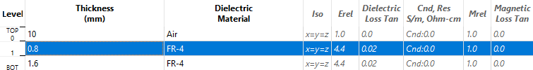
The a new FR-4 layer is added to the dielectric stackup. You should now have three dielectric layers, as shown below:
Each time a new dielectric layer is added, a corresponding level is also added to the bottom of the new dielectric layer.
You are now finished setting up your dielectric layers. At this point, you may wish to save your project. If you wish to do so, click OK, save your project, then select Edit > Circuit Settings to return to the Circuit Settings dialog box.
Tech Layers
Tech Layers allow you to define a group of polygons with common properties including the level on which they are placed. This enables you to more easily control a large group of polygons and make changes to them as efficiently as possible. Tech Layers provide uses and advantages similar to drawing layers in CAD and EDA programs.
In this tutorial, you will create two Planar Tech Layers: one for the main spiral inductor metal and one for the underpass. In addition you need to create a Via Tech Layer that connects the underpass to the main spiral inductor metal.
Main Spiral Inductor Tech Layer
First, you will create a Planar Tech Layer for the main spiral inductor metal.
Click the [Tech Layers] button in the left pane of the Circuit Settings dialog box.
The Tech Layers pane is displayed, providing you with a list of available Tech Layers. Since you started with a blank project, only one Tech Layer is in the list (Planar1). You will modify this Tech Layer and use it for the main spiral inductor metal.
Select the pre-existing Tech Layer and click the Edit button.
The Tech Layer Properties dialog box appears.
Enter "Spiral" for the new name of the Tech Layer.
Any name is acceptable, but it must be a unique name.
The level number should already be set to level 0, so you do not need to change it.
As explained earlier in this tutorial, level 0 is the top-most level. A thick layer of air and the top cover are above this level.
Select Copper (annealed) from the Conductor drop-down list.
You created this conductor material earlier in this tutorial.
The Metal Model should already be set to Thin Metal, so you do not need to change it.
The Metal Model determines how Sonnet will model the metal thickness (i.e., the z-direction). A Thin Metal polygon is modeled as a 2D sheet of zero thickness. For more information about the Thin Metal model and other metal models, see Metal Models.
Enter a Thickness of "0.042".
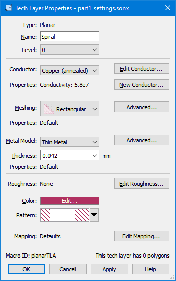
The 0.042 mm thickness represents the combination of ½ oz. copper (0.017 mm) and additional metal plating (0.025 mm). The properties should now look like this:
Optionally, change the Color and/or Pattern.
The color and pattern are used for display purposes only. You may change them at any time without affecting the EM analysis.
Click OK to save your changes.
Your spiral Tech Layer is now finished.
Underpass Tech Layer
Next, you will create a similar Tech Layer for the underpass metal.
Click the Add Planar button.
The Tech Layer Properties dialog box appears.
Enter "Underpass" for the name of the Tech Layer.
Any name is acceptable, but it must be a unique name.
Change the level number to "1".
Level 1 corresponds to the level below level 0.
Select Copper (annealed) from the Conductor drop-down list.
This is the same conductor material as the main spiral inductor metal.
The Metal Model should already be set to Thin Metal, so you do not need to change it.
This Tech Layer will use the same Metal Model as the main spiral Tech Layer.
Enter a Thickness of "0.017".
The 0.017 mm thickness corresponds to the thickness of ½ oz copper. The properties should now look like this:
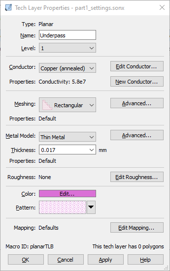
Optionally, change the Color and/or Pattern.
The color and pattern are used for display purposes only.
Click OK to save your changes.
Your underpass Tech Layer is now finished. You should now see two Tech Layers in the Tech Layers list.
Via Tech Layer
Next, you will create a Via Tech Layer that will be used to connect the main spiral metal to the underpass.
Click the  Add Via button.
The Tech Layer Properties dialog box appears.
Enter "Vias" for the name of the Tech Layer.
Any name is acceptable, but it must be a unique name.
Set the Begin level number to "0" and the End level number to 1.
Any via assigned to this Tech Layer will go from level 0 (the main spiral metal) to level 1 (the underpass).
The Begin and End values may be interchanged with no affect on the EM results. For example, if you had set the Begin level to 1 and the End level to 0, the EM solver would compute the same results.
Select Copper (annealed) from the Conductor drop-down list.
This is the same conductor material as the main spiral inductor metal and the underpass.
The Meshing should already be set to Ring, so you do not need to change it.
Ring meshing is the default meshing for new Via Tech Layers and is the recommended meshing for modeling most solid and hollow vias at DC and RF. The via polygon is modeled as a one cell wide wall of via subsections and is hollow in the middle, containing no metal. This meshing adequately models solid vias at RF because most of the current travels along the perimeter of the via. For more information on via meshing options, see Meshing.
In the Metal Model section, click the Advanced button.
The Model Properties dialog box appears. The Metal Model determines the cross-sectional area used to compute the loss of a via.
Unselect the Solid checkbox.
Enter a Wall Thickness of "0.025".
The 0.025 mm thickness corresponds to the metal plating thickness of the via.
Click OK to save your changes.
Your Advanced Metal Model settings are saved. The properties should now look like this:
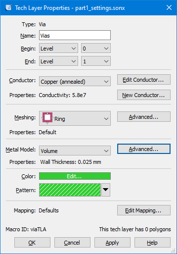
Optionally, change the Color and/or Pattern.
The color and pattern are used for display purposes only.
Click OK to save your changes.
Your Via Tech Layer is now finished.
You are now finished with setting up your Tech Layers. At this point, you may wish to save your project. If you wish to do so, click OK, save your project, then select Edit > Circuit Settings to return to the Circuit Settings dialog box.
Analysis Plan
You will now define the frequencies at which you wish to perform the analysis. For this tutorial, you will sweep the frequency from 0.1 GHz to 2.0 GHz using and an Adaptive Sweep. An Adaptive Sweep uses the Adaptive Band Synthesis (ABS) technique to provide results for a large number of frequency points by performing an EM analysis at only a small number of discrete frequencies. To learn more about ABS sweeps, see Adaptive Band Synthesis.
Click the Analysis Plan button.
The Analysis Plan pane is displayed. The Analysis Plan pane allows you to set up frequency sweeps, parameter sweeps, or optimization for your project. You will use it to set up your frequency sweep. An unspecified ABS sweep is already displayed in Sweep Set 1.
Double-click the line "ABS: Please double click to set up this sweep."
The ABS sweep requires two entries: one for the start frequency, and one for the stop frequency.
Enter 0.1 and 2.0 for the ABS start and stop frequencies.
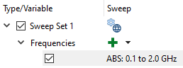
Your Analysis Plan is now complete. For information on more complex sweeps, see Analysis Plan Overview.
EM Options
You will now set up the options for the EM Solver.
Click the EM Options button.
The EM Options pane is displayed.
Select the Compute currents checkbox.
Selecting the Compute currents checkbox instructs the EM solver to calculate and save current density data which can be viewed using the Current Density Viewer. Please be aware that calculating current density data can increase the time needed for your analysis. For an Adaptive (ABS) Sweep, current density data is only calculated for discrete data points.
Click the Advanced drop-down caret to display the Advanced section of the EM Options pane.
You may skip this step if the Advanced section is already displayed.
The De-embed checkbox is selected by default and should remain selected, even when your circuit does not contain reference planes. De-embedding negates the fringing fields surrounding a port. See De-embedding Overview for more details.
In the Advanced section, click the Configure ABS tab.
This tab allows you to make changes that affect the ABS algorithm.
Select the Q-Factor accuracy checkbox.
By default, the ABS algorithm uses S-parameters as the criteria for convergence. The Q-Factor Accuracy run option adds the Q-factor of your analysis as a criterion for convergence. This results in a more accurate Q-factor but may require more discrete frequencies to be analyzed before convergence is reached. Since we will be plotting the Q-factor, this is an important option to enable.
Click OK to apply your changes.
Your changes are applied and the Circuit Settings dialog box is closed.
Save Your Progress
You have completed the Circuit Settings portion of this tutorial, so you should save your project now.
Select File > Save to save all your changes.
The project is saved as "part1_settings.sonx".